CDB5361 Cirrus Logic Inc, CDB5361 Datasheet - Page 3
CDB5361
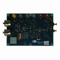
Manufacturer Part Number
CDB5361
Description
BOARD EVAL FOR CS5361 STEREO ADC
Manufacturer
Cirrus Logic Inc
Specifications of CDB5361
Number Of Adc's
2
Number Of Bits
24
Sampling Rate (per Second)
192k
Data Interface
Serial
Inputs Per Adc
1 Differential
Power (typ) @ Conditions
198mW @ 5 V
Voltage Supply Source
Analog and Digital
Operating Temperature
-10°C ~ 70°C
Utilized Ic / Part
CS5361
Product
Audio Modules
Lead Free Status / RoHS Status
Contains lead / RoHS non-compliant
Lead Free Status / RoHS Status
Lead free / RoHS Compliant, Contains lead / RoHS non-compliant
Other names
598-1547


LIST OF FIGURES
LIST OF TABLES
DS467F2
Figure 1. Single Speed Mode Stopband Rejection ..................................................... 8
Figure 2. Single Speed Mode Transition Band ........................................................... 8
Figure 3. Single Speed Mode Transition Band (Detail) .............................................. 8
Figure 4. Single Speed Mode Passband Ripple ......................................................... 8
Figure 5. Double Speed Mode Stopband Rejection ................................................... 8
Figure 6. Double Speed Mode Transition Band ......................................................... 8
Figure 7. Double Speed Mode Transition Band (Detail) ............................................. 9
Figure 8. Double Speed Mode Passband Ripple ....................................................... 9
Figure 9. Quad Speed Mode Stopband Rejection ...................................................... 9
Figure 10. Quad Speed Mode Transition Band .......................................................... 9
Figure 11. Quad Speed Mode Transition Band (Detail) ............................................. 9
Figure 12. Quad Speed Mode Passband Ripple ........................................................ 9
Figure 13. Master Mode, Left Justified SAI .............................................................. 12
Figure 14. Slave Mode, Left Justified SAI ................................................................ 12
Figure 15. Master Mode, I
Figure 16. Slave Mode, I
Figure 17. OVFL Output Timing ............................................................................... 12
Figure 18. Left Justified Serial Audio Interface ......................................................... 13
Figure 19. I
Figure 20. OVFL Output Timing, I2S Format ............................................................ 13
Figure 21. OVFL Output Timing, Left-Justified Format ............................................. 13
Figure 22. Typical Connection Diagram ................................................................... 15
Figure 23. CS5361 Master Mode Clocking ............................................................... 17
Figure 24. CS5361 Recommended Analog Input Buffer .......................................... 18
Table 1. CS5361 Mode Control .............................................................................. 16
Table 2. CS5361 Slave Mode Clock Ratios ........................................................... 16
Table 3. CS5361 Common Master Clock Frequencies .......................................... 17
Table 4. Revision History ....................................................................................... 23
2
S Serial Audio Interface ........................................................................ 13
2
S SAI ................................................................................ 12
2
S SAI .............................................................................. 12
CS5361
3
Related parts for CDB5361
Image
Part Number
Description
Manufacturer
Datasheet
Request
R

Part Number:
Description:
Development Kit
Manufacturer:
Cirrus Logic Inc
Datasheet:
Part Number:
Description:
Development Kit
Manufacturer:
Cirrus Logic Inc
Datasheet:


Part Number:
Description:
High-efficiency PFC + Fluorescent Lamp Driver Reference Design
Manufacturer:
Cirrus Logic Inc
Datasheet:
Part Number:
Description:
Development Kit
Manufacturer:
Cirrus Logic Inc
Datasheet:
Part Number:
Description:
Development Kit
Manufacturer:
Cirrus Logic Inc
Datasheet:

Part Number:
Description:
Development Kit
Manufacturer:
Cirrus Logic Inc
Datasheet:
Part Number:
Description:
Development Kit
Manufacturer:
Cirrus Logic Inc
Datasheet:
Part Number:
Description:
Development Kit
Manufacturer:
Cirrus Logic Inc
Datasheet:
Part Number:
Description:
Development Kit
Manufacturer:
Cirrus Logic Inc
Datasheet:

Part Number:
Description:
EVALUATION BOARD FOR CS8427
Manufacturer:
Cirrus Logic Inc
Datasheet:

Part Number:
Description:
BOARD EVAL FOR CS8416 RCVR
Manufacturer:
Cirrus Logic Inc
Datasheet:

Part Number:
Description:
EVALUATION BOARD FOR CS8420
Manufacturer:
Cirrus Logic Inc
Datasheet:

Part Number:
Description:
KIT DEVELOPMENT EP9315 ARM9
Manufacturer:
Cirrus Logic Inc
Datasheet:

Part Number:
Description:
KIT DEVELOPMENT EP9302 ARM9
Manufacturer:
Cirrus Logic Inc
Datasheet: