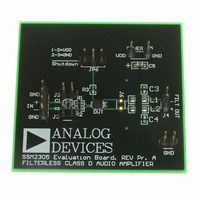
SSM2305-EVALZ Analog Devices Inc, SSM2305-EVALZ Datasheet - Page 12
SSM2305-EVALZ
Manufacturer Part Number
SSM2305-EVALZ
Description
BOARD EVAL FOR SSM2305 LFCSP
Manufacturer
Analog Devices Inc
Specifications of SSM2305-EVALZ
Amplifier Type
Class D
Output Type
1-Channel (Mono)
Max Output Power X Channels @ Load
2.8W x 1 @ 4 Ohm
Voltage - Supply
2.2 V ~ 5.5 V
Operating Temperature
-40°C ~ 85°C
Board Type
Fully Populated
Utilized Ic / Part
SSM2305
Silicon Manufacturer
Analog Devices
Application Sub Type
Audio Power Amplifier - Class D
Kit Application Type
Amplifier
Silicon Core Number
SSM2305
Kit Contents
Board
Lead Free Status / RoHS Status
Lead free / RoHS Compliant


SSM2305
GAIN
The SSM2305 has a default gain of 18 dB that can be reduced by
using a pair of external resistors with a value calculated as follows:
POP-AND-CLICK SUPPRESSION
Voltage transients at the output of audio amplifiers can occur when
shutdown activates or deactivates. Voltage transients as low as
10 mV can be heard as audio pops in the speaker. Clicks and
pops can also be classified as undesirable audible transients gener-
ated by the amplifier system and, therefore, as not coming from
the system input signal. Such transients can be generated when
the amplifier system changes its operating mode. For example, the
following can be sources of audible transients: system power-up/
power-down, mute/unmute, input source change, and sample rate
change. The SSM2305 has a pop-and-click suppression architecture
that reduces these output transients, resulting in noiseless activation
and deactivation.
OUTPUT MODULATION DESCRIPTION
The SSM2305 uses three-level, Σ-Δ output modulation. Each
output is able to swing from GND to VDD, and vice versa. Ideally,
when no input signal is present, the output differential voltage is
0 V because there is no need to generate a pulse. In a real-world
situation, there are always noise sources present. Due to this
constant presence of noise, a differential pulse generates when it
is required in response to this stimulus. A small amount of current
flows into the inductive load when the differential pulse is
generated. However, most of the time output differential voltage is
0 V due to the Analog Devices patented three-level, Σ-Δ output
modulation. This feature ensures that the current flowing through
the inductive load is small.
When the user wants to send an input signal, an output pulse is
generated to follow the input voltage. The differential pulse density
is increased by raising the input signal level. Figure 34 depicts
three-level, Σ-Δ output modulation with and without input stimuli.
VOUT
VOUT
VOUT
OUT+
OUT–
OUT+
OUT–
OUT+
OUT–
Figure 34. 3-Level, Σ-Δ Output Modulation with and Without Input Stimuli
External Gain Settings = 296 kΩ/(37 kΩ + R
OUTPUT = 0V
OUTPUT > 0V
OUTPUT < 0V
EXT
)
+5V
0V
+5V
0V
+5V
0V
–5V
+5V
0V
+5V
0V
+5V
0V
+5V
0V
+5V
0V
0V
–5V
Rev. A | Page 12 of 16
LAYOUT
As output power continues to increase, care needs to be taken
to lay out PCB traces and wires properly between the amplifier,
load, and power supply. A good practice is to use short, wide
PCB tracks to decrease voltage drops and minimize inductance.
Ensure that track widths are at least 200 mil for every inch of
track length for lowest dc resistance (DCR), and use 1 oz or 2 oz
of copper PCB traces to further reduce IR drops and inductance.
A poor layout increases voltage drops, consequently affecting
efficiency. Use large traces for the power supply inputs and
amplifier outputs to minimize losses due to parasitic trace
resistance.
Proper grounding guidelines help improve audio performance,
minimize crosstalk between channels, and prevent switching noise
from coupling into the audio signal. To maintain high output swing
and high peak output power, the PCB traces that connect the
output pins to the load and supply pins should be as wide as
possible to maintain the minimum trace resistances. It is also
recommended that a large ground plane be used for minimum
impedances.
In addition, good PCB layouts isolate critical analog paths from
sources of high interference. Separate high frequency circuits
(analog and digital) from low frequency circuits.
Properly designed multilayer PCBs can reduce EMI emission
and increase immunity to the RF field by a factor of 10 or more
compared with double-sided boards. A multilayer board allows
a complete layer to be used for the ground plane, whereas the
ground plane side of a double-sided board is often disrupted with
signal crossover.
If the system has separate analog and digital ground and power
planes, place the analog ground plane underneath the analog
power plane, and, similarly, place the digital ground plane
underneath the digital power plane. There should be no overlap
between analog and digital ground planes or analog and digital
power planes.
INPUT CAPACITOR SELECTION
The SSM2305 does not require input coupling capacitors if the
input signal is biased from 1.0 V to V
are required if the input signal is not biased within this recom-
mended input dc common-mode voltage range, if high-pass
filtering is needed, or if using a single-ended source. If high-pass
filtering is needed at the input, the input capacitor, together with
the input resistor of the SSM2305, forms a high-pass filter
whose corner frequency is determined by the following
equation:
The input capacitor can significantly affect the performance of
the circuit. Not using input capacitors degrades both the output
offset of the amplifier and the dc PSRR performance.
f
C
= 1/(2π × R
IN
× C
IN
)
DD
− 1.0 V. Input capacitors
Related parts for SSM2305-EVALZ
Image
Part Number
Description
Manufacturer
Datasheet
Request
R

Part Number:
Description:
±1.7g Dual-Axis IMEMS Accelerometer Evaluation Board
Manufacturer:
Analog Devices Inc
Datasheet:

Part Number:
Description:
Inertial Sensor Evaluation System
Manufacturer:
Analog Devices Inc
Datasheet:
Part Number:
Description:
Manufacturer:
Analog Devices Inc
Datasheet:
Part Number:
Description:
Manufacturer:
Analog Devices Inc
Datasheet:
Part Number:
Description:
Manufacturer:
Analog Devices Inc
Datasheet:
Part Number:
Description:
Manufacturer:
Analog Devices Inc
Datasheet:
Part Number:
Description:
Manufacturer:
Analog Devices Inc
Datasheet:
Part Number:
Description:
Manufacturer:
Analog Devices Inc
Datasheet:
Part Number:
Description:
Manufacturer:
Analog Devices Inc
Datasheet:
Part Number:
Description:
Manufacturer:
Analog Devices Inc
Datasheet:
Part Number:
Description:
Manufacturer:
Analog Devices Inc
Datasheet:
Part Number:
Description:
Manufacturer:
Analog Devices Inc
Datasheet:
Part Number:
Description:
Manufacturer:
Analog Devices Inc
Datasheet: