STEVAL-CCA002V1 STMicroelectronics, STEVAL-CCA002V1 Datasheet - Page 28
STEVAL-CCA002V1
Manufacturer Part Number
STEVAL-CCA002V1
Description
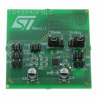
BOARD EVAL FOR LP DIFF TS4994IQT
Manufacturer
STMicroelectronics
Specifications of STEVAL-CCA002V1
Design Resources
STEVAL-CCA002V1 Gerber Files
Amplifier Type
Class AB
Output Type
1-Channel (Mono)
Max Output Power X Channels @ Load
1W x 1 @ 8 Ohm
Voltage - Supply
2.5 V ~ 5.5 V
Operating Temperature
-40°C ~ 85°C
Board Type
Fully Populated
Utilized Ic / Part
TS4994
Description/function
Audio Amplifiers
Operating Supply Voltage
2.5 V to 5.5 V
Output Power
1 W
Product
Audio Modules
Silicon Manufacturer
ST Micro
Silicon Core Number
TS4994
Kit Application Type
Amplifier
Application Sub Type
Audio Power Amplifier
Kit Contents
Board
Rohs Compliant
Yes
Lead Free Status / RoHS Status
Lead free / RoHS Compliant
For Use With/related Products
TS4994
Other names
497-6395
STEVAL-CCA002V1
STEVAL-CCA002V1


Application information
4.8
4.9
28/35
To calculate the maximum ambient temperature T
●
●
●
Example: V
Using the power dissipation formula given above in
T
Equation 5
Therefore, the maximum allowable value for T
Decoupling of the circuit
Two capacitors are needed to correctly bypass the TS4994. A power supply bypass
capacitor C
C
indirect influence on power supply disturbances. With a value for C
similar THD+N performance to that shown in the datasheet.
In the high frequency region, if C
on the power supply rail are less filtered.
On the other hand, if C
more filtered.
C
result of PSRR (with input grounded and in the lower frequency region).
Wake-up time: t
When the standby is released to put the device ON, the bypass capacitor C
immediately. As C
properly until the C
time or t
TS4994 gain is close to zero. After the wake-up time, the gain is released and set to its
nominal value.
If C
wake-up time.
amb
s
b
has particular influence on the THD+N in the high frequency region (above 7kHz) and an
has an influence on THD+N at lower frequencies, but its function is critical to the final
b
The value of the power supply voltage, V
The value of the load resistor, R
The R
P
T
has a value other than 1µF, refer to the graph in
is calculated as follows:
amb
dissmax
WU
= 125-80x0.633=74°C
thja
s
and is specified in
CC
and a bias voltage bypass capacitor
= 633mW
value for the package type
= 5V, R
b
b
is directly linked to the bias of the amplifier, the bias will not work
voltage is correct. The time to reach this voltage is called the wake-up
L
s
WU
= 8Ω, R
is higher than 1µF, the disturbances on the power supply rail are
T
Table 3 on page
amb
thja
s
is lower than 1µF, it increases THD+N, and disturbances
=
= 80°C/W
L
125° C R
–
amb
CC
6, with C
TJHA
amb
C
is:
b
Equation 3
×
.
Figure 69 on page 20
allowable, you need to know:
P
dissmax
b
=1µF. During the wake-up time, the
this gives a result of:
s
of 1µF, you can expect
b
to establish the
is not charged
TS4994
Related parts for STEVAL-CCA002V1
Image
Part Number
Description
Manufacturer
Datasheet
Request
R

Part Number:
Description:
EVAL BOARD CC DRVR HI DENSE LEDS
Manufacturer:
STMicroelectronics
Datasheet:

Part Number:
Description:
EVAL BOARD CC DRVR HI DENSE LEDS
Manufacturer:
STMicroelectronics
Datasheet:

Part Number:
Description:
BATTERY CHARGER CELL PHONE
Manufacturer:
STMicroelectronics
Datasheet:

Part Number:
Description:
BOARD EVAL FOR MEMS SENSORS
Manufacturer:
STMicroelectronics
Datasheet:

Part Number:
Description:
KIT DEV STARTER ST10F276Z5
Manufacturer:
STMicroelectronics
Datasheet:

Part Number:
Description:
BOARD EVAL UPS 450W VOUT=220V
Manufacturer:
STMicroelectronics
Datasheet:

Part Number:
Description:
BOARD STLM75/STDS75/ST72F651
Manufacturer:
STMicroelectronics
Datasheet:

Part Number:
Description:
EVAL BOARD ENERGY METER MONO
Manufacturer:
STMicroelectronics
Datasheet:

Part Number:
Description:
EVAL BOARD ENERGY METER MONO
Manufacturer:
STMicroelectronics
Datasheet:

Part Number:
Description:
EVAL BOARD ENERGY METER MONO
Manufacturer:
STMicroelectronics
Datasheet:

Part Number:
Description:
STMicroelectronics [RIPPLE-CARRY BINARY COUNTER/DIVIDERS]
Manufacturer:
STMicroelectronics
Datasheet:
Part Number:
Description:
STMicroelectronics [LIQUID-CRYSTAL DISPLAY DRIVERS]
Manufacturer:
STMicroelectronics
Datasheet:
Part Number:
Description:
BOARD EVAL FOR MEMS SENSORS
Manufacturer:
STMicroelectronics
Datasheet: