STEVAL-CCA003V1 STMicroelectronics, STEVAL-CCA003V1 Datasheet - Page 22
STEVAL-CCA003V1
Manufacturer Part Number
STEVAL-CCA003V1
Description
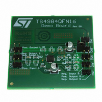
BOARD EVAL FOR LV TS4984IQT
Manufacturer
STMicroelectronics
Specifications of STEVAL-CCA003V1
Design Resources
STEVAL-CCA003V1 Gerber Files
Amplifier Type
Class AB
Output Type
2-Channel (Stereo)
Max Output Power X Channels @ Load
1W x 2 @ 8 Ohm
Voltage - Supply
2.2 V ~ 5.5 V
Operating Temperature
-40°C ~ 85°C
Board Type
Fully Populated
Utilized Ic / Part
TS4984
Description/function
Audio Amplifiers
Operating Supply Voltage
2.2 V to 5.5 V
Output Power
1 W
Product
Audio Modules
Silicon Manufacturer
ST Micro
Silicon Core Number
TS4984
Kit Application Type
Amplifier
Application Sub Type
Stereo Audio Power Amplifier
Kit Contents
Board
Rohs Compliant
Yes
Lead Free Status / RoHS Status
Lead free / RoHS Compliant
For Use With/related Products
TS4984
Other names
497-6396
STEVAL-CCA003V1
STEVAL-CCA003V1
Available stocks
Company
Part Number
Manufacturer
Quantity
Price


TS4984
4.5 Decoupling the circuit
Two capacitors are needed to correctly bypass the TS4984. A power supply bypass capacitor C
bias voltage bypass capacitor C
C
influence on power supply disturbances. With a value for C
performances to those shown in the datasheet. For example:
C
(with input grounded and in the lower frequency region), in the following manner:
Note that C
higher the PSRR.
4.6 Wake-up time, T
When the standby is released to put the device ON, the bypass capacitor C
immediately. As C
voltage is correct. The time to reach this voltage is called wake-up time or T
characteristics table with C
If C
value.
Due to process tolerances, the maximum value of wake-up time could be establish by the graph in
Figure
Note:
22/29
Figure 66: Typical wake-up time vs. C
S
b
has an influence on THD+N at lower frequencies, but its function is critical to the final result of PSRR
has particular influence on the THD+N in the high frequency region (above 7 kHz) and an indirect
b
In the high frequency region, if C
power supply rail are less filtered.
On the other hand, if C
filtered.
If C
If C
is substantial.
600
500
400
300
200
100
has a value other than 1 µF, please refer to the graph in
0
0.1
67.
b
b
Bypass capacitor C
refer to the previous graph (considering for example for C
Tamb=25 ° C
is higher than 1µF, the benefit on THD+N at lower frequencies is small, but the benefit to PSRR
is lower than 1µF, THD+N increases at lower frequencies and PSRR worsens.
in
has a non-negligible effect on PSRR at lower frequencies. The lower the value of C
1
Vcc=2.6V
Bypass Capacitor Cb ( F)
b
is directly linked to the bias of the amplifier, the bias will not work properly until the C
WU
2
b
as also a tolerance of typically +/-20%. To calculate the wake-up time with this tolerance,
b
S
= 1 µF.
Vcc=3.3V
is higher than 1 µF, those disturbances on the power supply rail are more
3
B
.
Vcc=5V
S
4
is lower than 1 µF, it increases THD+N and disturbances on the
b
4.7
Figure 67: Maximum wake-up time vs. C
600
500
400
300
200
100
b
0
0.1
= 1 µF in the range of 0.8 µF ≤ 1 µF ≤ 1.2 µF).
Tamb=25 ° C
S
of 1 µF, you can expect similar THD+N
Figure 66
1
Vcc=2.6V
Bypass Capacitor Cb ( F)
to establish the wake-up time
WU
2
Application Information
and specified in electrical
Vcc=3.3V
b
3
will not be charged
Vcc=5V
4
b
S
4.7
in
and a
, the
b
Related parts for STEVAL-CCA003V1
Image
Part Number
Description
Manufacturer
Datasheet
Request
R

Part Number:
Description:
EVAL BOARD CC DRVR HI DENSE LEDS
Manufacturer:
STMicroelectronics
Datasheet:

Part Number:
Description:
EVAL BOARD CC DRVR HI DENSE LEDS
Manufacturer:
STMicroelectronics
Datasheet:

Part Number:
Description:
BATTERY CHARGER CELL PHONE
Manufacturer:
STMicroelectronics
Datasheet:

Part Number:
Description:
BOARD EVAL FOR MEMS SENSORS
Manufacturer:
STMicroelectronics
Datasheet:

Part Number:
Description:
KIT DEV STARTER ST10F276Z5
Manufacturer:
STMicroelectronics
Datasheet:

Part Number:
Description:
BOARD EVAL UPS 450W VOUT=220V
Manufacturer:
STMicroelectronics
Datasheet:

Part Number:
Description:
BOARD STLM75/STDS75/ST72F651
Manufacturer:
STMicroelectronics
Datasheet:

Part Number:
Description:
EVAL BOARD ENERGY METER MONO
Manufacturer:
STMicroelectronics
Datasheet:

Part Number:
Description:
EVAL BOARD ENERGY METER MONO
Manufacturer:
STMicroelectronics
Datasheet:

Part Number:
Description:
EVAL BOARD ENERGY METER MONO
Manufacturer:
STMicroelectronics
Datasheet:

Part Number:
Description:
STMicroelectronics [RIPPLE-CARRY BINARY COUNTER/DIVIDERS]
Manufacturer:
STMicroelectronics
Datasheet:
Part Number:
Description:
STMicroelectronics [LIQUID-CRYSTAL DISPLAY DRIVERS]
Manufacturer:
STMicroelectronics
Datasheet:
Part Number:
Description:
BOARD EVAL FOR MEMS SENSORS
Manufacturer:
STMicroelectronics
Datasheet: