MCP1640EV-SBC Microchip Technology, MCP1640EV-SBC Datasheet - Page 13
MCP1640EV-SBC
Manufacturer Part Number
MCP1640EV-SBC
Description
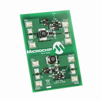
BOARD EVAL FOR MCP1640
Manufacturer
Microchip Technology
Type
DC/DC Switching Converters, Regulators & Controllersr
Datasheets
1.MCP1640CT-ICHY.pdf
(32 pages)
2.MCP1640CT-ICHY.pdf
(26 pages)
3.MCP1640EV-SBC.pdf
(22 pages)
Specifications of MCP1640EV-SBC
Main Purpose
DC/DC, Step Up
Outputs And Type
1, Non-Isolated
Voltage - Output
2V, 3.3V or 5V
Current - Output
100mA, 350mA
Voltage - Input
0.35 ~ 5.5V
Regulator Topology
Boost
Frequency - Switching
500kHz
Board Type
Fully Populated
Utilized Ic / Part
MCP1640
Input Voltage
0.35 V to 5.5 V
Output Voltage
3.3 V to 5 V
Operating Supply Voltage
0.35 V to 5.5 V
Product
Power Management Modules
Supply Current
300 mA
Kit Contents
Board
Features
Automatic PFM/PWM Operation, Enable State Selectable Using Mini-Dip Switch On Board
Svhc
No SVHC (15-Dec-2010)
Core Architecture
Power Management - Voltage Regulator
Rohs Compliant
Yes
For Use With/related Products
MCP1640
Lead Free Status / RoHS Status
Contains lead / RoHS non-compliant
Power - Output
-
Lead Free Status / Rohs Status
Lead free / RoHS Compliant
Available stocks
Company
Part Number
Manufacturer
Quantity
Price
Company:

Part Number:
MCP1640EV-SBC
Manufacturer:
Microchip Technology
Quantity:
135
Company:
Part Number:
MCP1640EV-SBC
Manufacturer:
MICROCHIP
Quantity:
12 000


2.2
© 2010 Microchip Technology Inc.
GETTING STARTED
The MCP1640 Single Quadruple-A Battery Boost Converter Reference Design is fully
assembled and tested to evaluate and demonstrate the MCP1640 products.
2.2.1
2.2.1.1
The MCP1640 Single Quadruple-A Battery Boost Converter Reference Design is
equipped with an innovative Energizer Battery Holder, which protects against the
reverse insertion of the AAAA alkaline battery. If the battery is inserted correctly, the
board will start in Standby mode. To switch the output ON, press the button S1 for 2
seconds. The output is active for approximately 25 seconds. Pressing the button during
this period will turn OFF the output.
Extra connectors are placed on the top side of board:
• TP1 and TP5 for positive (V
• TP2 and TP3 for negative (GND
These two connectors help engineers power the board from an external power supply.
In this case, the maximum input voltage should not exceed the 3.3V output
(V
greater than or equal to the output voltage.
The output connector is called “OUT”, and is referenced to GND. The maximum output
current is 130 mA when the board is powered by a quadruple-A alkaline battery, which
has a typical capacity of 600 mAh.
2.2.1.2
To test the board, follow the next steps:
1. Insert the quadruple-A battery in its holder, paying attention to respect the
2. Connect a voltmeter and a 47Ω/0.5W resistor, between “OUT” and “–”
3. Press and hold the push-button for approximately 2 seconds. The LED should be
4. The LED will be ON for approximately 25 seconds. During this period, verify the
5. Press and hold the push-button for 2 seconds to verify that power turns ON and
The resistor R9 is not populated. The component pads are provided for experimental
use. The header J3 is also not populated. It can be use to re-program the
microcontroller.
IN
polarity.
connectors, as shown in Figure 2-2.
lit.
presence of 3.3V at “OUT”.
OFF.
< V
OUT
Power Input and Output Connection
POWERING THE MCP1640 SINGLE QUADRUPLE-A BATTERY BOOST
CONVERTER REFERENCE DESIGN
BOARD TESTING
). The output voltage will not remain regulated for input voltages that are
IN
)
)
Installation and Operation
DS51922A-page 13
Related parts for MCP1640EV-SBC
Image
Part Number
Description
Manufacturer
Datasheet
Request
R

Part Number:
Description:
0.65V Start-up Synchronous Boost Regulator with True Output Disconnect or Input/Output Bypass Option
Manufacturer:
MICROCHIP [Microchip Technology]
Datasheet:

Part Number:
Description:
IC CONV DC-DC STEPUP SYNC 8DFN
Manufacturer:
Microchip Technology
Datasheet:

Part Number:
Description:
0.65v Start-up Synchronous Boost Regulator With True Output Disconnect Or Input/output Bypass Option
Manufacturer:
Microchip Technology Inc.
Datasheet:
Part Number:
Description:
Manufacturer:
Microchip Technology Inc.
Datasheet:
Part Number:
Description:
Manufacturer:
Microchip Technology Inc.
Datasheet:
Part Number:
Description:
Manufacturer:
Microchip Technology Inc.
Datasheet:
Part Number:
Description:
Manufacturer:
Microchip Technology Inc.
Datasheet:
Part Number:
Description:
Manufacturer:
Microchip Technology Inc.
Datasheet:
Part Number:
Description:
Manufacturer:
Microchip Technology Inc.
Datasheet:
Part Number:
Description:
Manufacturer:
Microchip Technology Inc.
Datasheet: