DM300023 Microchip Technology, DM300023 Datasheet - Page 9
DM300023
Manufacturer Part Number
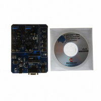
DM300023
Description
KIT DEMO DSPICDEM SMPS BUCK
Manufacturer
Microchip Technology
Series
dsPIC™r
Datasheets
1.AC164335.pdf
(286 pages)
2.DM300023.pdf
(22 pages)
3.DM300023.pdf
(18 pages)
4.DM300023.pdf
(50 pages)
5.DM300023.pdf
(16 pages)
Specifications of DM300023
Main Purpose
DC/DC, Step Down
Outputs And Type
2, Non-Isolated
Voltage - Input
7 ~ 15V
Regulator Topology
Buck
Board Type
Fully Populated
Utilized Ic / Part
dsPIC30F2020
Processor To Be Evaluated
dsPIC30F202x/1010
Interface Type
RS-232
Lead Free Status / RoHS Status
Lead free / RoHS Compliant
Current - Output
-
Voltage - Output
-
Power - Output
-
Frequency - Switching
-
Lead Free Status / Rohs Status
Lead free / RoHS Compliant
Available stocks
Company
Part Number
Manufacturer
Quantity
Price
Company:

Part Number:
DM300023
Manufacturer:
Microchip Technology
Quantity:
135
Company:
Part Number:
DM300023
Manufacturer:
MICROCHIP
Quantity:
12 000


13. Module: Output Compare Module
14. Module: Output Compare Module in PWM
© 2008 Microchip Technology Inc.
A glitch will be produced on an output compare pin
under the following conditions:
• The user software initially drives the I/O pin
• The output compare module is configured and
When these events occur, the output compare
module will drive the pin low for one instruction
cycle (T
Work around
None. However, the user may use a timer interrupt
and write to the associated PORT register to
control the pin manually.
The output compare module will miss a compare
event when the current duty cycle register
(OCxRS) value is 0x0000 (0% duty cycle) and the
OCxRS register is updated with a value of 0x0001.
The compare event is missed only the first time a
value of 0x0001 is written to OCxRS, and the
PWM output remains low for one PWM period.
Subsequent PWM high and low times occur as
expected.
Work around
None. If the current OCxRS register value is
0x0000, avoid writing a value of 0x0001 to
OCxRS. Instead, write a value of 0x0002;
however, in this case the duty cycle will be slightly
different from the desired value.
high using the output compare module or a
write to the associated PORT register.
enabled to drive the pin low at some later time
(OCxCON = 0x0002 or OCxCON = 0x0003).
CY
) after the module is enabled.
Mode
15. Module: SPI Module in Frame Master
16. Module: SPI Module in Slave Select Mode
Note:
Note:
dsPIC30F1010/202X
The SPI module will fail to generate frame
synchronization pulses when configured in the
Frame Master mode if the start of data is selected
to
synchronization pulse (FRMEN = 1, SPIFSD = 0).
However, the module functions correctly in Frame
Slave mode, and also in Frame Master mode if
FRMDLY = 0. This applies to the dsPIC30F2023
device only.
Work around
Manually drive the SSx pin (x = 1 or 2) high using
the associated PORT register, and then drive it low
after the required 1 bit-time pulse-width. This
operation needs to be performed when the
transmit buffer is written.
If FRMDLY = 0, no work around is needed.
The SPI module Slave Select functionality
(enabled by setting SSEN = 1) will not function
correctly. Whether the SSx pin (x = 1 or 2) is high
or low, the SPI data transfer will be completed and
an interrupt will be generated. This applies to the
dsPIC30F2023 device only.
Work around
Manually poll the SSx pin state in the SPI interrupt
by reading the associated PORT bit:
• If the PORT bit is ‘0’, then perform the required
• If the PORT bit is ‘1’, then clear the SPI
data read/write.
interrupt flag (SPIxIF), perform a dummy read
of the SPIxBUF register and return from the
Interrupt Service Routine.
coincide
The dsPIC30F1010/202X devices have
only one SPI. All references to x = 2 are
intended for software compatibility with
other dsPIC DSC devices.
The dsPIC30F1010/202X devices have
only one SPI. All references to x = 2 are
intended for software compatibility with
other dsPIC DSC devices.
Mode
with
the
start
DS80290J-page 9
of
the
frame
Related parts for DM300023
Image
Part Number
Description
Manufacturer
Datasheet
Request
R

Part Number:
Description:
Manufacturer:
Microchip Technology Inc.
Datasheet:
Part Number:
Description:
Manufacturer:
Microchip Technology Inc.
Datasheet:
Part Number:
Description:
Manufacturer:
Microchip Technology Inc.
Datasheet:
Part Number:
Description:
Manufacturer:
Microchip Technology Inc.
Datasheet:
Part Number:
Description:
Manufacturer:
Microchip Technology Inc.
Datasheet:
Part Number:
Description:
Manufacturer:
Microchip Technology Inc.
Datasheet:
Part Number:
Description:
Manufacturer:
Microchip Technology Inc.
Datasheet:
Part Number:
Description:
Manufacturer:
Microchip Technology Inc.
Datasheet: