DAK-85 Power Integrations, DAK-85 Datasheet - Page 7
DAK-85
Manufacturer Part Number
DAK-85
Description
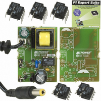
DESIGN ACCELERATOR KIT LP SWITCH
Manufacturer
Power Integrations
Series
LinkSwitch®-LPr
Specifications of DAK-85
Main Purpose
AC/DC, Primary Side
Outputs And Type
1, Isolated
Power - Output
2W
Voltage - Output
6V
Current - Output
330mA
Voltage - Input
90 ~ 265VAC
Regulator Topology
Flyback
Frequency - Switching
66kHz
Board Type
Bare (Unpopulated) and Fully Populated
Utilized Ic / Part
LNK562, LNK563, LNK564
Lead Free Status / RoHS Status
Lead free / RoHS Compliant
Other names
596-1104
Available stocks
Company
Part Number
Manufacturer
Quantity
Price
Company:

Part Number:
DAK-85
Manufacturer:
Power Integrations
Quantity:
135


Figure 7. Recommended Circuit Board Layout for LinkSwitch-LP using D Package (Assumes a HVDC Input Stage).
Output Diode
For best performance, the area of the loop connecting the
secondary winding, the output diode and the output fi lter
capacitor should be minimized. In addition, suffi cient copper
area should be provided at the anode and cathode terminals
of the diode for heat sinking. A larger area is preferred at the
quiet cathode terminal. A large anode area can increase high-
frequency radiated EMI.
Quick Design Checklist
As with any power supply design, all LinkSwitch-LP designs
should be verifi ed on the bench to make sure that component
specifi cations are not exceeded under worst-case conditions. The
following minimum set of tests is strongly recommended:
1. Maximum drain voltage – Verify that V
2. Maximum drain current – At maximum ambient
650 V at the highest input voltage and peak (overload) output
power. A 50 V margin to the 700 V BV
margin for design variation, especially in Clampless designs.
temperature, maximum input voltage and peak output
TOP VIEW
T r a n s f o r m e r
Output Filter
Capacitor
DSS
DS
specifi cation gives
does not exceed
OUT
DC
+
-
C
BP
FB
BP
3. Thermal Check – At specified maximum output
Design Tools
Up-to-date information on design tools can be found at the
Power Integrations web site: www.powerint.com.
D
(overload) power, verify drain current waveforms for any
signs of transformer saturation and excessive leading-edge
current spikes at startup. Repeat under steady state conditions
and verify that the leading-edge current spike event is below
I
maximum DRAIN current should be below the specifi ed
absolute maximum ratings.
power, minimum input voltage and maximum ambient
temperature, verify that the temperature specifi cations
are not exceeded for LinkSwitch-LP, transformer, output
diode and output capacitors. Enough thermal margin
should be allowed for part-to-part variation of the R
LinkSwitch-LP as specifi ed in the data sheet. Under low line
and maximum power, a maximum LinkSwitch-LP SOURCE pin
temperature of 100 °C is recommended to allow for
these variations.
LIMIT(MIN)
at the end of the t
S
S
S
S
Maximize hatched copper
areas (
heatsinking
LEB(MIN)
-
LNK562-564
HV DC
INPUT
) for optimum
. Under all conditions, the
+
PI-4582-021407
Input Filter
Capacitor
DS(ON)
Rev. H 11/08
7
of
Related parts for DAK-85
Image
Part Number
Description
Manufacturer
Datasheet
Request
R

Part Number:
Description:
KIT DESIGN ACCELERATOR MODEM
Manufacturer:
Power Integrations
Datasheet:

Part Number:
Description:
KIT DESIGN ACCELERATOR SET TOP
Manufacturer:
Power Integrations
Datasheet:

Part Number:
Description:
KIT REF DES DPA 6.6W DC-DC CONV
Manufacturer:
Power Integrations
Datasheet:

Part Number:
Description:
KIT DESIGN ACCELERATOR POE CONV
Manufacturer:
Power Integrations
Datasheet:

Part Number:
Description:
DESIGN ACCELERATOR KIT XT SWITCH
Manufacturer:
Power Integrations
Datasheet:

Part Number:
Description:
KIT DESIGN ACC PEAKSWITCH FAMILY
Manufacturer:
Power Integrations
Datasheet:

Part Number:
Description:
KIT DESIGN ACCELERATOR ADAPTER
Manufacturer:
Power Integrations
Datasheet:

Part Number:
Description:
KIT DESIGN ACCELERATOR ADAPTER
Manufacturer:
Power Integrations
Datasheet:

Part Number:
Description:
KIT DESIGN ACCELERATOR DC-DC
Manufacturer:
Power Integrations
Datasheet:

Part Number:
Description:
KIT DESIGN ACCELERATOR DPA SW
Manufacturer:
Power Integrations
Datasheet: