IRDC3621 International Rectifier, IRDC3621 Datasheet - Page 16
IRDC3621
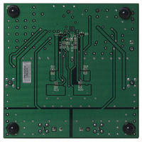
Manufacturer Part Number
IRDC3621
Description
BOARD EVAL DUAL SYNC BUCK CTRLR
Manufacturer
International Rectifier
Datasheet
1.IR3621MTR.pdf
(29 pages)
Specifications of IRDC3621
Main Purpose
DC/DC, Step Down
Outputs And Type
2, Non-Isolated
Voltage - Output
1.8V, 2.5V
Current - Output
10A, 10A
Voltage - Input
5.5 ~ 14.5V
Regulator Topology
Buck
Frequency - Switching
400kHz
Board Type
Fully Populated
Utilized Ic / Part
IR3621
Lead Free Status / RoHS Status
Lead free / RoHS Compliant
Power - Output
-


IR3621 & (PbF)
Cross Over Frequency:
The stability requirement will be satisfied by placing the
poles and zeros of the compensation network according
to following design rules. The consideration has been
taken to satisfy condition (16) regarding transconduc-
tance error amplifier.
These design rules will give a crossover frequency ap-
proximately one-tenth of the switching frequency. The
higher the band width, the potentially faster the load tran-
sient response. The DC gain will be large enough to pro-
vide high DC-regulation accuracy (typically -5dB to -12dB).
The phase margin should be greater than 45 for overall
stability.
Based on the frequency of the zero generated by ESR
versus crossover frequency, the compensation type can
be different. The table below shows the compensation
type and location of crossover frequency.
Type II (PI)
Type III (PID)
Method A
Type III (PID)
Method B
Details are dicussed in application Note AN-1043 which
can be downloaded from the IR Web-Site.
16
Compensator
Table - The compensation type and location of zero
F
Where:
V
V
Lo = Output Inductor
Co = Total Output Capacitors
O
IN
OSC
Type
= R
= Maximum Input Voltage
F
F
F
F
F
= Oscillator Ramp Voltage
P1
P2
P3
Z1
Z2
7
×C
=
=
= 0
=
=
2π×R
2π×R
2π×C
2π×R
10
×
Crossover Frequency
crossover frequency.
F
F
F
V
1
Location of Zero
1
LC
LC
LC
V
7
8
10
OSC
7
×C
×C
×
IN
< F
< F
< F
×(R
1
(
×
11
10
1
ESR
O
O
C
C
(F
< F
2π×Lo×Co
6
< f
12
12
+ R
< F
O
×C
+C
)
S
ESR
/2 < F
8
O
11
11
)
1
< f
< f
)
S
S
ZO
/2
/2
2π×C
2π×R
Electrolytic,
1
Capacitor
Tantalum,
10
Tantalum
---(17)
Ceramic
Ceramic
Typical
1
Output
×R
7
×C
6
12
www.irf.com
Compensation for Slave Error Amplfier for 2-Phase
Configuration
The slave error amplifier is a differential-input transcon-
ductance amplifier, in 2-phase configuration the main goal
for the slave feed back loop is to control the inductor
current to match the master's inductor current as well
provides highest bandwidth and adequate phase margin
for overall stability. The following analysis is valid for both
using external current sense resistor and using DCR of
inductors.
The transfer function of power stage is expressed by:
As shown the transfer function is a function of inductor
current.
The transfer function for the compensation network is
given by equation (19), when using a series RC circuit
as shown in Figure 17:
D(s) =
The loop gain function is:
H(s)=[G(s) × D(s) × R
H(s)=R
G(s) =
Where:
V
L
V
2
IN
OSC
= Output Inductor
= Input Voltage
Figure 17 - The PI compensation network
R
S2
= Oscillator Peak Voltage
×
S2
Ve(s)
I
Ve(s)
L2
× I
(
(s)
g
m
R
L2
R
×
S1
S2
(s)
=
Fb2
R
R
I
I
sL
=
L2
for slave channel.
L1
S1
S2
Vp2
(
)
2
g
×
× V
S2
V
m
L
L
×
IN
2
1
]
(
E/A2
1+sR
OSC
R
R
S1
S2
sC
)
2
2
×
C
Comp2
(
2
)
1 + sC
---(18)
×
R
C
sC
(
2
2
sL
2
Ve
2
2
R
×V
V
2
)
IN
OSC
---(19)
)
Related parts for IRDC3621
Image
Part Number
Description
Manufacturer
Datasheet
Request
R

Part Number:
Description:
SCHOTTKY RECTIFIER
Manufacturer:
International Rectifier Corp.
Datasheet:
Part Number:
Description:
SCHOTTKY RECTIFIER
Manufacturer:
International Rectifier Corp.
Datasheet:
Part Number:
Description:
SCHOTTKY RECTIFIER
Manufacturer:
International Rectifier Corp.
Datasheet:
Part Number:
Description:
SCHOTTKY RECTIFIER
Manufacturer:
International Rectifier Corp.
Datasheet:
Part Number:
Description:
SCHOTTKY RECTIFIER
Manufacturer:
International Rectifier Corp.
Datasheet:
Part Number:
Description:
SCHOTTKY RECTIFIER
Manufacturer:
International Rectifier Corp.
Datasheet:
Part Number:
Description:
SCHOTTKY RECTIFIER
Manufacturer:
International Rectifier Corp.
Datasheet:
Part Number:
Description:
SCHOTTKY RECTIFIER
Manufacturer:
International Rectifier Corp.
Datasheet:
Part Number:
Description:
SCHOTTKY RECTIFIER
Manufacturer:
International Rectifier Corp.
Datasheet:
Part Number:
Description:
SCHOTTKY RECTIFIER
Manufacturer:
International Rectifier Corp.
Datasheet:
Part Number:
Description:
SCHOTTKY RECTIFIER
Manufacturer:
International Rectifier Corp.
Datasheet:
Part Number:
Description:
SCHOTTKY RECTIFIER
Manufacturer:
International Rectifier Corp.
Datasheet:
Part Number:
Description:
SCHOTTKY RECTIFIER
Manufacturer:
International Rectifier Corp.
Datasheet:
Part Number:
Description:
SCHOTTKY RECTIFIER
Manufacturer:
International Rectifier Corp.
Datasheet:
Part Number:
Description:
SCHOTTKY RECTIFIER
Manufacturer:
International Rectifier Corp.
Datasheet: