LM5030EVAL National Semiconductor, LM5030EVAL Datasheet

EVALUATION BOARD FOR LM5030

LM5030EVAL

Manufacturer Part Number
LM5030EVAL
Description
EVALUATION BOARD FOR LM5030
Manufacturer
National Semiconductor
Series
PowerWise®r
Datasheets

Specifications of LM5030EVAL

Main Purpose
DC/DC, Step Down
Outputs And Type
1, Isolated
Voltage - Output
3.3V
Current - Output
10A
Voltage - Input
36 ~ 75V
Regulator Topology
Buck
Board Type
Fully Populated
Utilized Ic / Part
LM5030
Lead Free Status / RoHS Status
Not applicable / Not applicable
Power - Output
-
Frequency - Switching
-
Other names
*LM5030EVAL
© 2004 National Semiconductor Corporation
LM5030 Evaluation Board
Introduction
The LM5030EVAL evaluation board provides the design en-
gineer with a fully functional push-pull power converter using
the LM5030 PWM controller. The performance of the board
is as follows:
• Input range: 36V to 75V
• Output voltage: 3.3V
• Output current: 0 to 10A
• Measured efficiency: 82% (at 48V in, 10A Load Current)
• Board size: 2.4 x 2.4 x 0.5 inches
• Load regulation: ± 1.0% (1 - 10A)
• Line regulation: ± 0.15% (36 - 75V)
• Shutdown input
• Synchronizing input
The printed circuit board consists of 2 layers of 2 ounce
copper on FR4 material, with a total thickness of 0.062
inches. The board is designed for continuous operation at
rated load.
Theory Of Operation
Referring to Figure 7, the LM5030 controller (U1) alternately
drives two N channel MOSFETs, which feed the two halves
of the power transformer’s primary (T1). The transformer’s
secondary is rectified, and filtered with an LC filter (L2,
C3-5), to provide the output voltage. The feedback path
starts with the LM3411 precision regulator driver (U3) which
senses the output voltage, compares it to its internal refer-
ence, and drives an optocoupler (U2) based on the error
voltage. The optocoupler provides isolation in the feedback
path, and its open collector output drives the COMP pin on
the LM5030, which controls the pulse width to the MOS-
FETs. The lower the voltage at the COMP pin, the smaller
the MOSFET duty cycle.
Current in the main transformer’s primary is monitored at the
LM5030’s CS pin via a current sense transformer (T2). The
voltage at the CS pin is used for current mode PWM control
and current limit protection.
AN200892
National Semiconductor
Application Note 1305
Dennis Morgan
January 2004
The output inductor (L2) not only smoothes the output volt-
age waveform, but also generates an auxiliary voltage (by
means of its secondary winding) to power the Vcc pin on the
LM5030. This feature reduces power dissipation within the
IC, thereby increasing reliability.
A Synchronizing input pad (SYNC) is provided on the board
to synchronize the circuit’s operating frequency to an exter-
nal source. A Shutdown input pad (SD) permits shutting
down the circuit’s operation from an external switch to
ground.
Board Layout and Probing
The pictorial in Figure 1 shows the placement of the signifi-
cant components which may be probed in evaluating the
circuit’s operation. The following should be kept in mind
when using scope or meter probes:
1. The board has two circuit grounds - one associated with
2. The main current carrying components (L1, T1, T2, Q1,
3. Use care when probing the primary side at maximum
4. At maximum load current (10A), the wire size, and
5. The input voltage conector is J1.
the input power, and one associated with the output
power. The grounds are capacitively coupled (C6), but
are DC isolated.
Q2, D1 and L2) will be hot to the touch at maximum load
current. USE CAUTION. If operating at maximum load
current for extended periods, the use of a fan to provide
forced air flow is recommended.
input voltage. 75 volts is enough to produce shocks and
sparks.
length, used to connect the board’s output to the load
becomes important. Ensure there is not a significant
voltage drop in the wires. Note that two connectors are
provided at the output - one for the +3.3V output (J2
Out), and one for the Ground connection (J3 IGND). It is
advisable to make good use of this feature to ensure a
low loss connection.
www.national.com

Related parts for LM5030EVAL

LM5030EVAL Summary of contents

Page 1

... LM5030 Evaluation Board Introduction The LM5030EVAL evaluation board provides the design en- gineer with a fully functional push-pull power converter using the LM5030 PWM controller. The performance of the board is as follows: • Input range: 36V to 75V • Output voltage: 3.3V • Output current 10A • ...

Page 2

Board Layout and Probing Board Connections/Start-Up The input connection to the board from a power supply is made to connector J1. The power supply must be capable of supplying not only the current during normal operation, but also the inrush ...

Page 3

Performance (Continued) current, the output will be regulated to within the input voltage is varied over its range (36 - 75V). The power conversion efficiency is shown in Figure 3. Waveforms If the circuit ...

Page 4

FIGURE 3. Efficiency vs Load Current and V 4 20089203 IN ...

Page 5

OUT 36V 1.0A 2.2µS 5.3µS 266.7 48V 10A 1.9µS 5.5µS 270.3 75V 1.0A 1.2µS 6.2µS 270 10.5V 36V 72V 90V 10V 11.5V 48V 96V 130V 18V 10.5V 75V 150V ...

Page 6

FIGURE 6. Average Voltage at the CS pin vs Input Current www.national.com FIGURE 5. V Voltage vs Load Current CC 20089206 6 20089205 ...

Page 7

7 www.national.com ...

Page 8

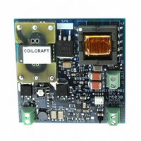
... Q1, 2 SUD19N20-90 J1-3 651-1727010 Note 1: Data sheets for L1, L2, and T1 are available from Coilcraft at http://www.coi1craft.com/prod_pwr.cfm. Select “Magnetics for National Semiconductor 100V Push-Pull Current Mode PWM Controller, LM5030”. Note 2: Data sheet for T2 is available from Pulse Engineering at http://www.pulseeng.com/default.cfm. www.national.com ...

Page 9

PCB Layout Diagrams FIGURE 8. Bottom Layer (viewed from top) 9 20089208 www.national.com ...

Page 10

PCB Layout Diagrams www.national.com (Continued) FIGURE 9. Top Silk Screen 10 20089209 ...

Page 11

... BANNED SUBSTANCE COMPLIANCE National Semiconductor certifies that the products and packing materials meet the provisions of the Customer Products Stewardship Specification (CSP-9-111C2) and the Banned Substances and Materials of Interest Specification (CSP-9-111S2) and contain no ‘‘Banned Substances’’ as defined in CSP-9-111S2. ...

Related keywords