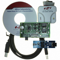
MULTIPHSPOL-RD Silicon Laboratories Inc, MULTIPHSPOL-RD Datasheet - Page 24
MULTIPHSPOL-RD
Manufacturer Part Number
MULTIPHSPOL-RD
Description
KIT REFERENCE DESIGN FOR SI825X
Manufacturer
Silicon Laboratories Inc
Type
Other Power Managementr
Specifications of MULTIPHSPOL-RD
Main Purpose
DC/DC, Step Down
Outputs And Type
1, Non-Isolated
Voltage - Output
3.3V
Current - Output
40A
Voltage - Input
10 ~ 15V
Regulator Topology
Buck
Frequency - Switching
391kHz
Board Type
Fully Populated
Utilized Ic / Part
SI8250, SI8251, SI8252
Input Voltage
10 V to 15 V
Output Voltage
3.3 V
Interface Type
USB
Product
Power Management Modules
Supply Current
10 A
For Use With/related Products
Si8250
Lead Free Status / RoHS Status
Contains lead / RoHS non-compliant
Power - Output
-
Lead Free Status / Rohs Status
Lead free / RoHS Compliant
Other names
336-1323


Si8250/1/2
7.1. Pin Functions
7.1.1. RST/C2CK
CPU reset or debug tool clock. Driving this pin low
resets the CPU. This pin is also clocked by the USB
debug adaptor during debug.
7.1.2. I
Input to the peak current detector for pulse-by-pulse
current limiting and overcurrent protection shutdown
control.
7.1.3. V
ADC1 inverting input. This is the voltage feedback input
for the Si8250. The maximum allowable signal is V
7.1.4. GND
Digital ground for the 32LQFP package and the main
ground for the 28MLP package.
7.1.5. GNDA
Analog ground for 32LQFP only.
7.1.6. V
Digital supply voltage for the 32LQFP package and
main supply voltage for the 28MLP package.
7.1.7. V
Analog supply for 32LQFP only.
7.1.8. P1.0/V
Programmable multifunction I/O pin. This pin can be
software-configured to be either a Port 1 digital input or
24
P0.5
P0.4
P0.3/XCLK
P0.2
P0.1
P0.0
PH6
PH5
PH4
V
GND
PH3
PH2
PH1
DD
PK
Name
SENSE
DD
DDA
IN
or AIN0
QFN-28
Pin #
17
18
19
20
21
22
23
24
25
26
27
28
—
—
LQFP-32
Table 17. Pin Descriptions (Continued)
Pin#
19
20
22
23
24
25
26
27
28
29
30
31
32
21
DOUT
DOUT
DOUT
DOUT
DOUT
DOUT
Type
D I/O
D I/O
D I/O
D I/O
D I/O
D I/O
AIN
AIN
REF
Rev. 1.0
.
output, or an ADC0 input at AMUX address 0. If used in
a non-isolated application, positive input supply voltage
must be tied to this input through a resistor divider and
anti-aliasing capacitor to minimize the frequencies
above fS/2 (100 kHz) to prevent aliasing. Isolated
applications may use this input as general-purpose
digital I/O or analog input.
7.1.9. P1.1 or AIN1–P1.7 or AIN7
Programmable multifunction I/O pins. These pins can
be software-configured to be a Port 1 digital input or
output, or an ADC0 input. P1.7 also serves as the
debug data input (C2D) and is used during debug by the
USB debug adaptor. P1.7 may be used as general-
purpose digital I/O when not in debug mode. Any of the
digital peripherals may be programmed to connect to
these pins.
7.1.10. P0.0–P0.7
Programmable multifunction I/O pins. These pins can
be software-configured to be either a Port 1 digital input
or output, or an ADC0 input. Any of the digital
peripherals (including the ENABLE input) may be
programmed to connect to these pins. P0.3 may be
programmed to serve as an external (25 MHz nominal)
clock input.
7.1.11. PH1–PH6
DPWM gate control (complementary drive) outputs.
These signals connect to the MOSFET gates through
an external gate driver. The output levels swing
between ground and V
Port 0 I/O
Port 0 I/O
Port 0 I/O
Port 0 I/O
Port 0 I/O
Port 0 I/O or bidirectional debug data
Phase 6 switch control output
Phase 5 switch control output
Phase 4 switch control output
Power supply input
Ground
Phase 3 switch control output
Phase 2 switch control output
Phase 1 switch control output
DD
Description
.
Related parts for MULTIPHSPOL-RD
Image
Part Number
Description
Manufacturer
Datasheet
Request
R

Part Number:
Description:
SMD/C°/SINGLE-ENDED OUTPUT SILICON OSCILLATOR
Manufacturer:
Silicon Laboratories Inc
Part Number:
Description:
Manufacturer:
Silicon Laboratories Inc
Datasheet:
Part Number:
Description:
N/A N/A/SI4010 AES KEYFOB DEMO WITH LCD RX
Manufacturer:
Silicon Laboratories Inc
Datasheet:
Part Number:
Description:
N/A N/A/SI4010 SIMPLIFIED KEY FOB DEMO WITH LED RX
Manufacturer:
Silicon Laboratories Inc
Datasheet:
Part Number:
Description:
N/A/-40 TO 85 OC/EZLINK MODULE; F930/4432 HIGH BAND (REV E/B1)
Manufacturer:
Silicon Laboratories Inc
Part Number:
Description:
EZLink Module; F930/4432 Low Band (rev e/B1)
Manufacturer:
Silicon Laboratories Inc
Part Number:
Description:
I°/4460 10 DBM RADIO TEST CARD 434 MHZ
Manufacturer:
Silicon Laboratories Inc
Part Number:
Description:
I°/4461 14 DBM RADIO TEST CARD 868 MHZ
Manufacturer:
Silicon Laboratories Inc
Part Number:
Description:
I°/4463 20 DBM RFSWITCH RADIO TEST CARD 460 MHZ
Manufacturer:
Silicon Laboratories Inc
Part Number:
Description:
I°/4463 20 DBM RADIO TEST CARD 868 MHZ
Manufacturer:
Silicon Laboratories Inc
Part Number:
Description:
I°/4463 27 DBM RADIO TEST CARD 868 MHZ
Manufacturer:
Silicon Laboratories Inc
Part Number:
Description:
I°/4463 SKYWORKS 30 DBM RADIO TEST CARD 915 MHZ
Manufacturer:
Silicon Laboratories Inc
Part Number:
Description:
N/A N/A/-40 TO 85 OC/4463 RFMD 30 DBM RADIO TEST CARD 915 MHZ
Manufacturer:
Silicon Laboratories Inc
Part Number:
Description:
I°/4463 20 DBM RADIO TEST CARD 169 MHZ
Manufacturer:
Silicon Laboratories Inc