NCP1012GEVB ON Semiconductor, NCP1012GEVB Datasheet - Page 8
NCP1012GEVB
Manufacturer Part Number
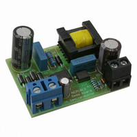
NCP1012GEVB
Description
EVAL BOARD FOR NCP1012G
Manufacturer
ON Semiconductor
Specifications of NCP1012GEVB
Design Resources
NCP1012 Eval Brd BOM NCP1012GEVB Gerber Files NCP1012 Eval Brd Schematic
Main Purpose
AC/DC, Primary Side
Outputs And Type
1, Isolated
Voltage - Output
12V
Voltage - Input
230VAC
Regulator Topology
Flyback
Frequency - Switching
100kHz
Board Type
Fully Populated
Utilized Ic / Part
NCP1012
Lead Free Status / RoHS Status
Lead free / RoHS Compliant
Current - Output
-
Power - Output
-
Lead Free Status / Rohs Status
Lead free / RoHS Compliant
For Use With/related Products
NCP1012G
Other names
NCP1012GEVBOS


Introduction
solution (actually an enhanced NCP1200 controller section)
together with a high- -voltage power MOSFET in a
monolithic structure. The component integrates everything
needed to build a rugged and low- -cost Switch- -Mode Power
Supply (SMPS) featuring low standby power. The Quick
Selection Table on Page 2, details the differences between
references, mainly peak current setpoints and operating
frequency.
No need for an auxiliary winding: ON Semiconductor
Very High Voltage Integrated Circuit technology lets you
supply the IC directly from the high- -voltage DC rail. We call
it Dynamic Self- -Supply (DSS). This solution simplifies the
transformer design and ensures a better control of the SMPS
in difficult output conditions, e.g. constant current
operations. However, for improved standby performance,
an auxiliary winding can be connected to the V
disable the DSS operation.
Short- -circuit protection: By permanently monitoring the
feedback line activity, the IC is able to detect the presence of
a short- -circuit, immediately reducing the output power for
a total system protection. Once the short has disappeared, the
controller resumes and goes back to normal operation.
Fail- -safe optocoupler and OVP: When an auxiliary
winding is connected to the V
internal Dynamic Self- -Supply and takes its operating power
from the auxiliary winding. A 8.7 V active clamp is
connected between V
injected in this clamp exceeds a level of 7.4 mA (typical),
the controller immediately latches off and stays in this
position until V
converter from the wall). By adjusting a limiting resistor in
series with the V
implement an overvoltage protection function, latching off
the circuit in case of broken optocoupler or feedback loop
problems.
Low standby- -power: If SMPS naturally exhibits a good
efficiency at nominal load, it begins to be less efficient when
the output power demand diminishes. By skipping unneeded
switching cycles, the NCP101X drastically reduces the
power wasted during light load conditions. An auxiliary
winding can further help decreasing the standby power to
extremely low levels by invalidating the DSS operation.
Typical measurements show results below 80 mW @
230 Vac for a typical 7.0 W universal power supply.
The NCP101X offers a complete current- -mode control
CC
cycles down to 3.0 V (e.g. unplugging the
CC
CC
terminal, it becomes possible to
and ground. In case the current
CC
pin, the device stops its
APPLICATION INFORMATION
CC
http://onsemi.com
pin to
8
No acoustic noise while operating: Instead of skipping
cycles at high peak currents, the NCP101X waits until the
peak current demand falls below a fixed 1/4 of the maximum
limit. As a result, cycle skipping can take place without
having a singing transformer You can thus select cheap
magnetic components free of noise problems.
SPICE model: A dedicated model to run transient
cycle- -by- -cycle simulations is available but also an
averaged version to help close the loop. Ready- -to- -use
templates can be downloaded in OrCAD’s PSpice, and
INTUSOFT’s IsSpice4 from ON Semiconductor web site,
NCP101X related section.
Dynamic Self- -Supply
outlet, the internal current source (typically 8.0 mA) is
biased and charges up the V
Once the voltage on this V
level (typically 8.5 V), the current source turns off and
pulses are delivered by the output stage: the circuit is awake
and activates the power MOSFET. Figure 13 details the
internal circuitry.
When the power supply is first powered from the mains
Figure 13. The Current Source Regulates V
*In fault condition
Vref OFF = 8.5 V
Vref ON = 7.5 V
Vref Latch = 4.7 V*
+
Vref
Internal Supply
+
--
by Introducing a Ripple
(8.7 V Typ.)
+200 mV
VCC
CC
OFF
CC
capacitor reaches the VCC
capacitor from the drain pin.
Startup Source
V
CC
Drain
+
CV
CC
CC
OFF
Related parts for NCP1012GEVB
Image
Part Number
Description
Manufacturer
Datasheet
Request
R

Part Number:
Description:
Self−Supplied Monolithic Switcher for Low Standby−Power Offline SMPS
Manufacturer:
ONSEMI [ON Semiconductor]
Datasheet:

Part Number:
Description:
ON Semiconductor [VOLTAGE REGULATOR]
Manufacturer:
ON Semiconductor
Datasheet:
Part Number:
Description:
357-036-542-201 CARDEDGE 36POS DL .156 BLK LOPRO
Manufacturer:
ON Semiconductor
Datasheet:
Part Number:
Description:
357-036-542-201 CARDEDGE 36POS DL .156 BLK LOPRO
Manufacturer:
ON Semiconductor
Datasheet:
Part Number:
Description:
357-036-542-201 CARDEDGE 36POS DL .156 BLK LOPRO
Manufacturer:
ON Semiconductor
Datasheet:
Part Number:
Description:
357-036-542-201 CARDEDGE 36POS DL .156 BLK LOPRO
Manufacturer:
ON Semiconductor
Datasheet:
Part Number:
Description:
357-036-542-201 CARDEDGE 36POS DL .156 BLK LOPRO
Manufacturer:
ON Semiconductor
Datasheet:
Part Number:
Description:
357-036-542-201 CARDEDGE 36POS DL .156 BLK LOPRO
Manufacturer:
ON Semiconductor
Datasheet:
Part Number:
Description:
357-036-542-201 CARDEDGE 36POS DL .156 BLK LOPRO
Manufacturer:
ON Semiconductor
Datasheet:
Part Number:
Description:
357-036-542-201 CARDEDGE 36POS DL .156 BLK LOPRO
Manufacturer:
ON Semiconductor
Datasheet:
Part Number:
Description:
357-036-542-201 CARDEDGE 36POS DL .156 BLK LOPRO
Manufacturer:
ON Semiconductor
Datasheet:
Part Number:
Description:
357-036-542-201 CARDEDGE 36POS DL .156 BLK LOPRO
Manufacturer:
ON Semiconductor
Datasheet:
Part Number:
Description:
Manufacturer:
ON Semiconductor
Datasheet:
Part Number:
Description:
Manufacturer:
ON Semiconductor
Datasheet: