NCP5424EVB ON Semiconductor, NCP5424EVB Datasheet - Page 2
NCP5424EVB
Manufacturer Part Number
NCP5424EVB
Description
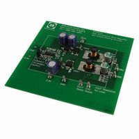
EVAL BOARD FOR NCP5424
Manufacturer
ON Semiconductor
Specifications of NCP5424EVB
Design Resources
NCP5424 Demo Board BOM NCP5424EVB Gerber Files NCP5424EVB Schematic
Main Purpose
DC/DC, Step Down
Outputs And Type
1, Non-Isolated
Voltage - Output
1.5V
Current - Output
17A
Voltage - Input
3.3V, 5V, 12V
Regulator Topology
Buck
Frequency - Switching
300kHz
Board Type
Fully Populated
Utilized Ic / Part
NCP5424
Lead Free Status / RoHS Status
Lead free / RoHS Compliant
Power - Output
-
Lead Free Status / Rohs Status
Lead free / RoHS Compliant
For Use With/related Products
NCP5424
Other names
NCP5424EVBOS


2.0 Test Configuration
3.0 Procedure
3.1 Configure equipment as shown in Figure 1. Set current limits for DC
supplies as listed in section 1.0.
3.2 Turn on power supplies in the following order: 12 V, 5 V, 3.3 V. Verify that
input currents do not exceed current limits.
3.3 Apply 17 A constant current electronic load or resistive load as described in
section 1.0. Verify that output maintains 1.5 V ±10% while under load.
3.4 Ground oscilloscope to any GND and probe switch nodes on 3.3 V and 5 V
sides. Verify that switching frequency is 300 kHz ±10% and that there is no
excessive jitter.
3.5 Remove load. Briefly short VOUT to GND. Verify that board does not
destabilize while shorted (no hissing, squealing, or excessive heat dissipation).
3.6 Turn off power supplies in the following order: 3.3 V, 5 V, 12 V.
Figure 1. NCP5424EVB Test Configuration.
Related parts for NCP5424EVB
Image
Part Number
Description
Manufacturer
Datasheet
Request
R

Part Number:
Description:
Dual Synchronous Buck Controller
Manufacturer:
ON Semiconductor
Datasheet:
Part Number:
Description:
ON Semiconductor [VOLTAGE REGULATOR]
Manufacturer:
ON Semiconductor
Datasheet:
Part Number:
Description:
357-036-542-201 CARDEDGE 36POS DL .156 BLK LOPRO
Manufacturer:
ON Semiconductor
Datasheet:
Part Number:
Description:
357-036-542-201 CARDEDGE 36POS DL .156 BLK LOPRO
Manufacturer:
ON Semiconductor
Datasheet:
Part Number:
Description:
357-036-542-201 CARDEDGE 36POS DL .156 BLK LOPRO
Manufacturer:
ON Semiconductor
Datasheet:
Part Number:
Description:
357-036-542-201 CARDEDGE 36POS DL .156 BLK LOPRO
Manufacturer:
ON Semiconductor
Datasheet:
Part Number:
Description:
357-036-542-201 CARDEDGE 36POS DL .156 BLK LOPRO
Manufacturer:
ON Semiconductor
Datasheet:
Part Number:
Description:
357-036-542-201 CARDEDGE 36POS DL .156 BLK LOPRO
Manufacturer:
ON Semiconductor
Datasheet:
Part Number:
Description:
357-036-542-201 CARDEDGE 36POS DL .156 BLK LOPRO
Manufacturer:
ON Semiconductor
Datasheet:
Part Number:
Description:
357-036-542-201 CARDEDGE 36POS DL .156 BLK LOPRO
Manufacturer:
ON Semiconductor
Datasheet:
Part Number:
Description:
357-036-542-201 CARDEDGE 36POS DL .156 BLK LOPRO
Manufacturer:
ON Semiconductor
Datasheet:
Part Number:
Description:
357-036-542-201 CARDEDGE 36POS DL .156 BLK LOPRO
Manufacturer:
ON Semiconductor
Datasheet:
Part Number:
Description:
Manufacturer:
ON Semiconductor
Datasheet:
Part Number:
Description:
Manufacturer:
ON Semiconductor
Datasheet: