MCP1650DM-DDSC1 Microchip Technology, MCP1650DM-DDSC1 Datasheet - Page 10
MCP1650DM-DDSC1
Manufacturer Part Number
MCP1650DM-DDSC1
Description
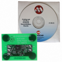
BOARD DEMO FOR MCP1650 SEPIC
Manufacturer
Microchip Technology
Type
DC/DC Switching Converters, Regulators & Controllersr
Specifications of MCP1650DM-DDSC1
Main Purpose
DC/DC, Step Up or Down
Outputs And Type
1, Non-Isolated
Voltage - Output
5V
Current - Output
160mA
Voltage - Input
3 ~ 7V
Regulator Topology
Boost
Frequency - Switching
750kHz
Board Type
Fully Populated
Utilized Ic / Part
MCP1650
Input Voltage
3 V to 7 V
Output Voltage
5 V
Product
Power Management Modules
For Use With/related Products
MCP1650R-E/MS
Lead Free Status / RoHS Status
Contains lead / RoHS non-compliant
Power - Output
-
Lead Free Status / Rohs Status
Lead free / RoHS Compliant


MCP1650/51/52/53
Note: Unless otherwise indicated,
I
FIGURE 2-19:
Current (Load Regulation).
FIGURE 2-20:
Input Voltage.
FIGURE 2-21:
Input Voltage.
DS21876A-page 10
OUT
= 10 mA, L = 3.3 µH, SHDN > V
12.17
12.16
12.15
12.14
12.13
12.12
12.11
12.10
1.230
1.225
1.220
1.215
1.210
1.205
0.26
0.24
0.22
0.20
0.18
0.16
0.14
0.12
0.10
2.7
10
2
3.0
2.5
20
3.3 3.6
30
V
3
IN
Output Current (mA)
T
= 4.3V
Output Voltage vs. Output
Output Voltage Ripple vs.
LBI Threshold Voltage vs.
V
J
40
Input Voltage (V)
Input Voltage (V)
IN
= - 40°C
3.9 4.2
3.5
= 3.3V
T
I
J
OUT
= +25°C
50
= 100mA
4
T
4.5
J
60
= +125°C
IH
4.5
, T
4.8 5.1
V
70
IN
A
= +25°C.
= 3.3V, VOUT = 12V, C
5
80
T
5.4
T
A
A
= +25°C
= +25°C
5.5
90
5.7 6.0
100
6
IN
= 10 µF (x5R or X7R Ceramic), C
FIGURE 2-22:
Input Voltage.
FIGURE 2-23:
LBO Sink Current.
FIGURE 2-24:
129
128
127
126
125
124
123
122
121
120
250
200
150
100
50
0
2
0
2.5
2
3
LBO Sink Current (mA)
T
T
T
J
J
J
LBI Hysteresis Voltage vs.
LBO Output Voltage vs.
LBO Output Timing.
= +125°C
= - 40°C
Input Votlage (V)
= +25°C
3.5
T
4
2004 Microchip Technology Inc.
T
J
J
= +125°C
= - 40°C
4
OUT
= 10 µF (X5R or X7R),
6
4.5
5
T
8
J
= +25°C
5.5
10
6
Related parts for MCP1650DM-DDSC1
Image
Part Number
Description
Manufacturer
Datasheet
Request
R

Part Number:
Description:
BOARD DEMO FOR MCP1650 WHITE LED
Manufacturer:
Microchip Technology
Datasheet:

Part Number:
Description:
BOARD DEMO FOR MCP165X
Manufacturer:
Microchip Technology
Datasheet:

Part Number:
Description:
Manufacturer:
Microchip Technology Inc.
Datasheet:
Part Number:
Description:
Manufacturer:
Microchip Technology Inc.
Datasheet:
Part Number:
Description:
Manufacturer:
Microchip Technology Inc.
Datasheet:
Part Number:
Description:
Manufacturer:
Microchip Technology Inc.
Datasheet:
Part Number:
Description:
Manufacturer:
Microchip Technology Inc.
Datasheet:
Part Number:
Description:
Manufacturer:
Microchip Technology Inc.
Datasheet:
Part Number:
Description:
Manufacturer:
Microchip Technology Inc.
Datasheet:
Part Number:
Description:
Manufacturer:
Microchip Technology Inc.
Datasheet: