MCP1256/7/8/9EV Microchip Technology, MCP1256/7/8/9EV Datasheet - Page 11
MCP1256/7/8/9EV
Manufacturer Part Number
MCP1256/7/8/9EV
Description
BOARD EVAL FOR MCP1256/7/8/9
Manufacturer
Microchip Technology
Specifications of MCP1256/7/8/9EV
Main Purpose
DC/DC, Step Up
Outputs And Type
1, Non-Isolated
Voltage - Output
3.3V
Current - Output
100mA
Voltage - Input
1.6 ~ 3.6V
Regulator Topology
Buck-Boost
Frequency - Switching
650kHz
Board Type
Fully Populated
Utilized Ic / Part
MCP1256, MCP1257, MCP1258, MCP1259
Processor To Be Evaluated
MCP1256/7/8/9
Lead Free Status / RoHS Status
Not applicable / Not applicable
Power - Output
-
Lead Free Status / RoHS Status
Lead free / RoHS Compliant, Not applicable / Not applicable


2.1
2.2
© 2006 Microchip Technology Inc.
INTRODUCTION
FEATURES
Chapter 2. Installation and Operation
The MCP1256/7/8/9 Charge Pump Evaluation Board demonstrates Microchip’s
MCP1256/7/8/9 devices. The MCP1256/7/8/9 devices are positive regulated charge
pumps that accept an input voltage from +1.8V to +3.6V and convert it to a regulated
3.3V output voltage. The MCP1256/7/8/9 provide a low-cost, compact and simple
solution for step-up DC/DC conversions, primarily in battery applications that do not
want to use switching regulator solutions because of EMI noise and inductor size.
The MCP1256/7/8/9 are designed to offer the highest possible efficiency under
common operating conditions, i.e. V
fixed switching frequency, 650 kHz (typically), allows for easy external filtering.
The MCP1256/7 provide a unique SLEEP mode feature. SLEEP mode reduces the
current drawn from the input supply while maintaining a regulated bias on external
peripherals. SLEEP mode can substantially increase battery run-time in portable
applications.
The MCP1258/9 provide a unique BYPASS mode feature. BYPASS virtually eliminates
the current drawn from the input supply by the device, while maintaining an unregulated
bias on external peripherals. BYPASS connects the input supply voltage to the output.
All remaining functions of the device are shutdown. BYPASS mode can substantially
increase battery run-time in portable applications.
The devices supply up to 100 mA of output current for input voltages, V
or equal to 2.2V.
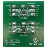
The MCP1256/7/8/9 Charge Pump Evaluation Board is used to evaluate various device
options. Two evaluation circuits are provided as a guide to external component
selection and board layout. Emphasis has been placed on cost, board area, thermal
management and performance. One evaluation circuit utilizes the MCP1256,
demonstrating the SLEEP mode feature along with a power good indication. The other
evaluation circuit utilizes the MCP1259 demonstrating the unique BYPASS mode
feature along with a low-battery indication.
The MCP1256/7/8/9 Charge Pump Evaluation Board has the following features:
• Evaluation of the MCP1256 in a 10-pin MSOP package
• Evaluation of the MCP1259 in a 10-pin MSOP package
• Simple, stand-alone operation
• Powered from external bench supply or compatible battery input
• Surface-mount design
• Fully assembled and tested
EVALUATION BOARD USER’S GUIDE
MCP1256/7/8/9 CHARGE PUMP
IN
= 2.4V or 2.8V, V
OUT
= 3.3V, I
OUT
IN
DS51603A-page 7
, greater than
= 100 mA. A
Related parts for MCP1256/7/8/9EV
Image
Part Number
Description
Manufacturer
Datasheet
Request
R

Part Number:
Description:
IC CHARGE PUMP DC/DC CONV 10DFN
Manufacturer:
Microchip Technology
Datasheet:

Part Number:
Description:
IC CHARGE PUMP DC/DC CONV 10MSOP
Manufacturer:
Microchip Technology
Datasheet:
Part Number:
Description:
IC CHARGE PUMP DC/DC CONV 10DFN
Manufacturer:
Microchip Technology
Datasheet:
Part Number:
Description:
IC CHARGE PUMP DC/DC CONV 10MSOP
Manufacturer:
Microchip Technology
Datasheet:

Part Number:
Description:
Regulated 3.3V, Low-Ripple Charge Pump with Low-Operating Current SLEEP Mode or BYPASS Mode
Manufacturer:
Microchip Technology
Datasheet:
Part Number:
Description:
Low Noise positive Regulator pump w/low power SLEEP mode, -40C to +85C, 10-MSOP, TUBE
Manufacturer:
Microchip Technology
Datasheet:

Part Number:
Description:
Manufacturer:
Microchip Technology Inc.
Datasheet:
Part Number:
Description:
Manufacturer:
Microchip Technology Inc.
Datasheet:
Part Number:
Description:
Manufacturer:
Microchip Technology Inc.
Datasheet:
Part Number:
Description:
Manufacturer:
Microchip Technology Inc.
Datasheet:
Part Number:
Description:
Manufacturer:
Microchip Technology Inc.
Datasheet:
Part Number:
Description:
Manufacturer:
Microchip Technology Inc.
Datasheet: