MCP1630DM-DDBS1 Microchip Technology, MCP1630DM-DDBS1 Datasheet - Page 13
MCP1630DM-DDBS1
Manufacturer Part Number
MCP1630DM-DDBS1
Description
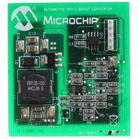
BOARD DEMO BOOST AUTO INPUT
Manufacturer
Microchip Technology
Type
DC/DC Switching Converters, Regulators & Controllersr
Specifications of MCP1630DM-DDBS1
Main Purpose
DC/DC, Step Up
Outputs And Type
1, Non-Isolated
Voltage - Output
36.5V
Current - Output
400mA
Voltage - Input
9 ~ 18V
Regulator Topology
Boost
Frequency - Switching
500kHz
Board Type
Fully Populated
Utilized Ic / Part
MCP1630
Silicon Manufacturer
Microchip
Silicon Core Number
MCP1630, PIC12F683
Core Architecture
PIC
Core Sub-architecture
PIC12
Silicon Family Name
Piccolo
Product
Power Management Modules
Lead Free Status / RoHS Status
Not applicable / Not applicable
Power - Output
-
Lead Free Status / Rohs Status
Lead free / RoHS Compliant
For Use With/related Products
MCP1630, PIC12F683
Lead Free Status / RoHS Status
Lead free / RoHS Compliant, Not applicable / Not applicable


© 2007 Microchip Technology Inc.
2.3.1.2
A variable resistive load can be used to verify the line and load regulation. The load
resistance is connected between the points TP3 and TP4. To measure the output
voltage, connect the common point of a multimeter to TP4 and the positive terminal to
TP3. By varying the load, the load regulation can be verified by measuring the output
voltage over the entire load range of 0 mA to 400 mA. Similarly, the line regulation can
be calculated by varying the line voltage from 9V to 18V and checking the output
voltage.
Evaluating the Application
The best way to evaluate the MCP1630 is to dig into the circuit and measure voltages
and currents with a Digital Voltage Meter (DVM) and probe the board with an
oscilloscope.
The firmware program in the PIC12F683 can also be edited to modify the operation of
the application.
Firmware
The PIC12F683 comes pre-programmed with firmware to operate the system as
described above. The file listing and firmware flow diagram are shown in Appendix
C. “Demo Board Firmware”.
The program is fairly simple and straight forward. There is an initialization routine at the
beginning of the program.
The TRISIO register controls the direction of GPIO pins, and is configured to set GP2
(oscillator pulses to the MCP1630/V) and GP5 (V
output port.
The Capture/Compare/PWM (CCP) module contains a 16-bit register which can
operate in PWM mode. The PWM period can be calculated by writing to the PR2
register. The PWM duty cycle is specified by writing to the CCPR1L register and to the
CCP1CON <5:4> bits. Up to 10-bit resolution is available. The CCPR1L contains the
eight MSbs and the CCP1CON <5:4> contains the two LSbs. This 10-bit value is
represented by CCPR1L:CCP1CON<5:4>. The switching frequency is set to 500 kHz.
The user can obtain different output voltages by programming the MCU to obtain
different V
Programming
Header J1 is provided for in-circuit programming. This is an optional feature since the
MCP1630 Automotive Input Boost Converter Demo Board comes pre-programmed
with firmware to operate the system. The PIC12F683 can be reprogrammed with the
Baseline Flash Microcontroller Programmer (BFMP).
REF
APPLY LOAD TO MCP1630 AUTOMOTIVE INPUT BOOST CONVERTER
DEMO BOARD
voltages.
REF
voltage to MCP1630/V) as an
DS51608B-page 9
Related parts for MCP1630DM-DDBS1
Image
Part Number
Description
Manufacturer
Datasheet
Request
R

Part Number:
Description:
BOARD CONV DEMO MCP1630 TRPL-OUT
Manufacturer:
Microchip Technology
Datasheet:

Part Number:
Description:
BOARD DEMO FOR MCP1630
Manufacturer:
Microchip Technology
Datasheet:

Part Number:
Description:
BOARD DEMO MCP1630 BIAS SUPPLY
Manufacturer:
Microchip Technology
Datasheet:

Part Number:
Description:
BOARD DEMO BOOST COUPLED INDUCTR
Manufacturer:
Microchip Technology
Datasheet:

Part Number:
Description:
BOARD DEM MCP1630 BOOST MODE LED
Manufacturer:
Microchip Technology
Datasheet:

Part Number:
Description:
Manufacturer:
Microchip Technology Inc.
Datasheet:
Part Number:
Description:
Manufacturer:
Microchip Technology Inc.
Datasheet:
Part Number:
Description:
Manufacturer:
Microchip Technology Inc.
Datasheet:
Part Number:
Description:
Manufacturer:
Microchip Technology Inc.
Datasheet:
Part Number:
Description:
Manufacturer:
Microchip Technology Inc.
Datasheet:
Part Number:
Description:
Manufacturer:
Microchip Technology Inc.
Datasheet: