MCP1630DM-DDBS1 Microchip Technology, MCP1630DM-DDBS1 Datasheet - Page 7
MCP1630DM-DDBS1
Manufacturer Part Number
MCP1630DM-DDBS1
Description
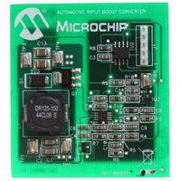
BOARD DEMO BOOST AUTO INPUT
Manufacturer
Microchip Technology
Type
DC/DC Switching Converters, Regulators & Controllersr
Specifications of MCP1630DM-DDBS1
Main Purpose
DC/DC, Step Up
Outputs And Type
1, Non-Isolated
Voltage - Output
36.5V
Current - Output
400mA
Voltage - Input
9 ~ 18V
Regulator Topology
Boost
Frequency - Switching
500kHz
Board Type
Fully Populated
Utilized Ic / Part
MCP1630
Silicon Manufacturer
Microchip
Silicon Core Number
MCP1630, PIC12F683
Core Architecture
PIC
Core Sub-architecture
PIC12
Silicon Family Name
Piccolo
Product
Power Management Modules
Lead Free Status / RoHS Status
Not applicable / Not applicable
Power - Output
-
Lead Free Status / Rohs Status
Lead free / RoHS Compliant
For Use With/related Products
MCP1630, PIC12F683
Lead Free Status / RoHS Status
Lead free / RoHS Compliant, Not applicable / Not applicable


AC/DC CHARACTERISTICS (CONTINUED)
TEMPERATURE SPECIFICATIONS
© 2005 Microchip Technology Inc.
Electrical Specifications: Unless otherwise noted, V
V
Current Sense Input
Maximum Current Sense Signal
MCP1630
Delay From CS to V
MCP1630
Maximum Current Sense Signal
MCP1630V
Delay From CS to V
MCP1630V
Minimum Duty Cycle
Current Sense Input Bias Current
Internal Driver
R
R
V
V
Protection Features
Under Voltage Lockout
Under Voltage Lockout Hysteresis UVLO
Thermal Shutdown
Thermal Shutdown Hysteresis
Note 1:
Electrical Specifications: V
Temperature Ranges
Operating Junction Temperature Range
Storage Temperature Range
Maximum Junction Temperature
Thermal Package Resistances
Thermal Resistance, 8L-DFN
(2 mm x 3 mm)
Thermal Resistance, 8L-MSOP
IN
EXT
EXT
DSON
DSON
for typical values = 5.0V, T
Rise Time
Fall Time
2:
3:
P-channel
N-channel
Parameters
Capable of higher frequency operation depending on minimum and maximum duty cycles needed.
External oscillator input (OSC IN) rise and fall times between 10 ns and 10 µs used for characterization testing. Signal
levels between 0.8V and 2.0V with rise and fall times measured between 10% and 90% of maximum and minimum
values. Not production tested.
The reference input of the internal amplifier is capable of rail-to-rail operation.
Parameters
EXT
EXT
IN
A
= 3.0V to 5.5V, F
= -40°C to +125°C.
T
T
T
V
V
R
R
SHD_HYS
CS_VEXT
CS_VEXT
DC
UVLO
CS_MAX
CS_MAX
T
T
I
DSon_P
DSon_N
T
Sym
CS_B
RISE
FALL
SHD
MIN
HYS
Sym
T
T
T
JA
JA
OSC
A
A
J
0.85
2.55
Min
2.7
50
—
—
—
—
—
—
—
—
—
—
= 1 MHz with 10% Duty Cycle, C
IN
= 3.0V to 5.5V, F
Min
-40
-65
—
—
—
17.5
-0.1
Typ
150
0.9
2.7
5.9
6.2
12
10
75
18
—
—
7
50.8
Typ
208
—
—
—
MCP1630/MCP1630V
OSC
Max
0.95
2.85
150
3.0
25
35
—
30
30
18
18
—
—
0
+125
+150
+150
Max
= 1 MHz with 10% Duty Cycle, C
—
—
Units
Units
IN
°C/W
°C/W
mV
µA
°C
°C
ns
ns
ns
ns
%
V
V
V
°C
°C
°C
= 0.1 µF. T
Set by maximum error amplifier
clamp voltage, divided by 3.
V
Maximum CS input range limited by
comparator input common mode
range. V
V
V
V
C
Typical for V
C
Typical for V
V
UVLO
Steady state
Transient
Typical 4-layer board with two
interconnecting vias
Typical 4-layer board
IN
FB
CS
IN
IN
L
L
= 100 pF
= 100 pF
> 4.25V
= 5V
falling, V
= V
= GND
A
= -40°C to +125°C.
REF
CS_MAX
+ 0.1V,
IN
IN
EXT
Conditions
Conditions
= 3V
= 3V
IN
= V
low state when in
= 0.1 µF,
DS21896B-page 7
IN
-1.4V
Related parts for MCP1630DM-DDBS1
Image
Part Number
Description
Manufacturer
Datasheet
Request
R

Part Number:
Description:
BOARD CONV DEMO MCP1630 TRPL-OUT
Manufacturer:
Microchip Technology
Datasheet:

Part Number:
Description:
BOARD DEMO FOR MCP1630
Manufacturer:
Microchip Technology
Datasheet:

Part Number:
Description:
BOARD DEMO MCP1630 BIAS SUPPLY
Manufacturer:
Microchip Technology
Datasheet:

Part Number:
Description:
BOARD DEMO BOOST COUPLED INDUCTR
Manufacturer:
Microchip Technology
Datasheet:

Part Number:
Description:
BOARD DEM MCP1630 BOOST MODE LED
Manufacturer:
Microchip Technology
Datasheet:

Part Number:
Description:
Manufacturer:
Microchip Technology Inc.
Datasheet:
Part Number:
Description:
Manufacturer:
Microchip Technology Inc.
Datasheet:
Part Number:
Description:
Manufacturer:
Microchip Technology Inc.
Datasheet:
Part Number:
Description:
Manufacturer:
Microchip Technology Inc.
Datasheet:
Part Number:
Description:
Manufacturer:
Microchip Technology Inc.
Datasheet:
Part Number:
Description:
Manufacturer:
Microchip Technology Inc.
Datasheet: