DAK-68A Power Integrations, DAK-68A Datasheet - Page 6
DAK-68A
Manufacturer Part Number
DAK-68A
Description
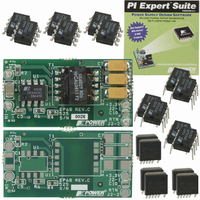
KIT DESIGN ACCELERATOR POE CONV
Manufacturer
Power Integrations
Series
DPA-Switch®r
Specifications of DAK-68A
Main Purpose
Special Purpose DC/DC, Power Over Ethernet
Outputs And Type
1, Non-Isolated
Power - Output
6.6W
Voltage - Output
3.3V
Current - Output
2A
Voltage - Input
36 ~ 57V
Regulator Topology
Flyback
Frequency - Switching
400kHz
Board Type
Bare (Unpopulated) and Fully Populated
Utilized Ic / Part
DPA423, DPA424, DPA425
Lead Free Status / RoHS Status
Not applicable / Not applicable
Other names
596-1007


4 Circuit Description
The Flyback topology was used to minimize circuit board size, parts count and cost, while
attaining excellent operating efficiency across the input voltage range.
4.1 DPA-Switch Primary
The DPA423G IC provides PWM control, startup, feedback, under/over voltage and over-
temperature protection functions. The integrated 220 V MOSFET provides excellent
switching characteristics at the selected 400 kHz operating frequency. The MOSFET and
controller consume minimal power, enabling a typical operating efficiency of 74%-78%
across the operating input voltage range (see Figure 7).
R1 provides a 25 kΩ input impedance, consistent with PoE Class 0 requirements. Above
30 V, Zener VR1 conducts, allowing n-channel MOSFET Q1 to turn on. Zener diode VR2
protects the gate of Q1 from overvoltage damage.
repeatable on and off timing.
Resistor R5 programs the typical input under-voltage ON threshold to 33 VDC. Resistors
R4 and R6 program the internal device current limit to reduce with increasing input
voltage. Maximum output (overload) current varies less than 5% across the operating
voltage range. The reduction in overload output current reduces secondary transformer
leakage spikes and allows the use of a 30 V Schottky diode, for the output rectifier D1.
The primary-side Zener clamp, VR3, provides protection of the DPA423G drain under
input surge and overvoltage conditions. Zener diode VR3 does not conduct under normal
operating conditions.
The primary bias winding provides CONTROL pin current after start-up. Diode D2
rectifies the bias winding, while components R8 and C11 reduce the high frequency
switching noise and reduce the peak charging of the bias voltage.
The DPA423G operates well within the recommended junction temperature limits
(100 °C) at an elevated ambient of 50 °C, in a free-convection cooled environment (see
Section 11).
4.2 Output Rectification
Schottky output diode D1 enables low-loss rectification of the secondary winding voltage.
Low ESR tantalum output capacitors, C7-9, reduce switching ripple and minimize losses.
Secondary output choke L1 and ceramic output capacitor C10 reduce high frequency
noise and ripple at the output.
Power Integrations
Tel: +1 408 414 9200 Fax: +1 408 414 9201
www.powerint.com
Resistors R2 and R3 provide
Page 6 of 28
Related parts for DAK-68A
Image
Part Number
Description
Manufacturer
Datasheet
Request
R

Part Number:
Description:
KIT DESIGN ACCELERATOR MODEM
Manufacturer:
Power Integrations
Datasheet:

Part Number:
Description:
KIT DESIGN ACCELERATOR SET TOP
Manufacturer:
Power Integrations
Datasheet:

Part Number:
Description:
KIT REF DES DPA 6.6W DC-DC CONV
Manufacturer:
Power Integrations
Datasheet:

Part Number:
Description:
DESIGN ACCELERATOR KIT XT SWITCH
Manufacturer:
Power Integrations
Datasheet:

Part Number:
Description:
DESIGN ACCELERATOR KIT LP SWITCH
Manufacturer:
Power Integrations
Datasheet:

Part Number:
Description:
KIT DESIGN ACC PEAKSWITCH FAMILY
Manufacturer:
Power Integrations
Datasheet:

Part Number:
Description:
KIT DESIGN ACCELERATOR ADAPTER
Manufacturer:
Power Integrations
Datasheet:

Part Number:
Description:
KIT DESIGN ACCELERATOR ADAPTER
Manufacturer:
Power Integrations
Datasheet:

Part Number:
Description:
KIT DESIGN ACCELERATOR DC-DC
Manufacturer:
Power Integrations
Datasheet:

Part Number:
Description:
KIT DESIGN ACCELERATOR DPA SW
Manufacturer:
Power Integrations
Datasheet: