EVLVIP15L-5WSB STMicroelectronics, EVLVIP15L-5WSB Datasheet - Page 29
EVLVIP15L-5WSB
Manufacturer Part Number
EVLVIP15L-5WSB
Description
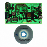
EVAL BOARD FOR VIPER 15
Manufacturer
STMicroelectronics
Series
VIPer™ plusr
Type
AC/DC Switching Convertersr
Datasheet
1.VIPER15LN.pdf
(40 pages)
Specifications of EVLVIP15L-5WSB
Main Purpose
AC/DC, Primary Side
Board Type
Fully Populated
Utilized Ic / Part
VIPer15
Product
Power Management Modules
Lead Free Status / RoHS Status
Lead free / RoHS Compliant
Current - Output
-
Voltage - Output
-
Voltage - Input
-
Power - Output
-
Frequency - Switching
-
Outputs And Type
-
Regulator Topology
-
Lead Free Status / Rohs Status
Lead free / RoHS Compliant
For Use With/related Products
VIPER15LN
Other names
497-9083


VIPER15
The time, from the high load detection, V
depends from the value of the capacitor C
OLP delay time can be calculating by the formula:
Equation 8
The current, I
also a part of the compensation loop , so they have to be selected taking into account the
proper delay and loop stability consideration. The
page 30
In the
circuit to compensate the feedback loop but also as element to delay the OLP shut down
owing to the time needed to charge the capacitor (see the
After the start-up time, t
capacitor could not be at its nominal value and the controller interpreter this situation as an
overload condition. In this case, the OLP delay helps to avoid an incorrect device shut down
during the start-up. See the relevant
Owing to the above considerations, the OLP delay time must be long enough to by-pass the
initial output voltage transient and check the overload condition only when the output voltage
is in steady state. The output transient time depends from the value of the output capacitor
and from the load.
When the value of the C
ensure enough OLP delay, an alternative compensation network can be used and it is
showed in
Using this alternative compensation network, two poles (f
introduced by the capacitors C
The capacitor C
is usually used to compensate the high frequency zero due to the ESR (Equivalent Series
Resistor) of the output capacitance of the fly-back converter.
The mathematical expressions of these poles and zero frequency, considering the scheme
in
Equation 9
Equation 10
Figure 35 on page 30
Figure 33 on page 27
show two different feedback networks.
Figure 35 on page 30
FB,
FB
is 3 μA as minimum value. The components connected to the FB pin are
introduces a pole (f
SU
FB
are reported by the equations below:
, during which the feedback voltage is fixed at V
capacitor calculated for the loop stability is too low and cannot
, the capacitor, C
T
f
PFB
OLP delay
Doc ID 15455 Rev 5
FB
.
and C
=
–
f
ZFB
2
Section 7.3 on page 16
⋅
PFB
⋅ π
FB1
=
=
FB
2
R
) at higher frequency than f
C
FB
C
FB
⋅
FB
and the resistor R
= V
⋅ π
FB
FB
(
and from the internal charge current, I
DYN
⋅
C
(
×
FBlin
, connected to FB pin is used as part of the
R
FB
1
V
--------------------------------------- -
)
FB
1
Figure 34 on page 30
+
FBolp
(
⋅
, to the overload turn-off, V
DYN
R
R
FB
FB
3μA
)
1
–
1
⋅
V
PFB
R
FBlin
FB
Equation 8
.
, f
1
FB1
)
PFB1
.
) and one zero (f
Operation description
ZB
).
and f
and
FBlin
PFB1
Figure 35 on
, the output
FB
. This pole
= V
FB
ZFB
FBolp
. The
) are
29/40
,
Related parts for EVLVIP15L-5WSB
Image
Part Number
Description
Manufacturer
Datasheet
Request
R

Part Number:
Description:
STMicroelectronics [RIPPLE-CARRY BINARY COUNTER/DIVIDERS]
Manufacturer:
STMicroelectronics
Datasheet:
Part Number:
Description:
STMicroelectronics [LIQUID-CRYSTAL DISPLAY DRIVERS]
Manufacturer:
STMicroelectronics
Datasheet:

Part Number:
Description:
BOARD EVAL FOR MEMS SENSORS
Manufacturer:
STMicroelectronics
Datasheet:
Part Number:
Description:
NPN TRANSISTOR POWER MODULE
Manufacturer:
STMicroelectronics
Datasheet:
Part Number:
Description:
TURBOSWITCH ULTRA-FAST HIGH VOLTAGE DIODE
Manufacturer:
STMicroelectronics
Datasheet:
Part Number:
Description:
Manufacturer:
STMicroelectronics
Datasheet:
Part Number:
Description:
DIODE / SCR MODULE
Manufacturer:
STMicroelectronics
Datasheet:
Part Number:
Description:
DIODE / SCR MODULE
Manufacturer:
STMicroelectronics
Datasheet:
Part Number:
Description:
Search -----> STE16N100
Manufacturer:
STMicroelectronics
Datasheet:
Part Number:
Description:
Search ---> STE53NA50
Manufacturer:
STMicroelectronics
Datasheet:
Part Number:
Description:
NPN Transistor Power Module
Manufacturer:
STMicroelectronics
Datasheet:
Part Number:
Description:
DIODE / SCR MODULE
Manufacturer:
STMicroelectronics
Datasheet: