IRDC3812 International Rectifier, IRDC3812 Datasheet - Page 16
IRDC3812
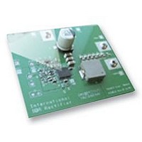
Manufacturer Part Number
IRDC3812
Description
BOARD EVAL SYNC BUCK CONVERTER
Manufacturer
International Rectifier
Specifications of IRDC3812
Silicon Manufacturer
International Rectifier
Kit Application Type
Power Management - Voltage Regulator
Application Sub Type
Synchronous Buck Converter
Features
Programmable Soft Start, Programmable
Rohs Compliant
Yes


11/04/08
Programming the Current-Limit
The Current-Limit threshold can be set by
connecting a resistor (R
low-side MOSFET to the OCSet pin. The
resistor can be calculated by using equation (3).
The
coefficient and it should be considered for the
worse case operation. This resistor must be
placed close to the IC, place a small ceramic
capacitor from this pin to power ground (PGnd)
for noise rejection purposes.
R
Where
υ
R
I
where
I
I
R
Note
Δ
Δ
I
SET
o
SET
DS(on)
SET
: i
i
OCSet
DS(on)
:
:
=
Temperatur
Max
Inductor
=
=
I =
V (
:
(I
(4A
=
=
Use
if
in
:
L(critical
:
o
Output
18mΩ
R
5V
-
∗
V
*
. 1
7
o
has
1.5)
24
=
)
) 5
is
)
=
ripple
∗
9.53KΩ
mΩ
used
V
+
R
e
∗
+
Current
in
υ
OCSet
D
Δ
2
0.97A
∗
R
i
V
=
ependency
for
a
L
current
o
DS(on)
for
18mΩ
∗
∗
low
F
I
OCSet
SET
V
s
=
positive
cc
6.97A
-
∗
) from drain of the
side
1
.5
-
=
-(3)
MOSFET
27mΩ
temperature
Layout Consideration
The layout is very important when designing high
frequency switching converters. Layout will affect
noise pickup and can cause a good design to
perform with less than expected results.
Start to place the power components, making all
the connection in the top layer with wide, copper
filled areas.
The inductor, output capacitor and the IR3812
should be as close to each other as possible.
This helps to reduce the EMI radiated by the
power traces due to the high switching currents
through them. Place the input capacitor directly to
the Vin pin of IR3812. To reduce the ESR replace
the single input capacitor with two parallel units.
The feedback part of the system should be kept
away from the inductor and other noise sources.
The
capacitors for Vcc and Vc should be close to their
respective pins. It is important to place the
feedback
resistors and compensation components close to
Fb and Comp pins.
In a multilayer PCB use one layer as a power
ground plane and have a control circuit ground
(analog ground), to which all signals are
referenced. The goal is to localize the high
current path to a separate loop that does not
interfere with the more sensitive analog control
function. These two grounds must be connected
together on the PC board layout at a single point.
The Power QFN is a thermally enhanced
package. Based on thermal performance it is
recommended to use at least a 4-layers PCB. To
effectively remove heat from the device the
exposed pad should be connected to the ground
plane using vias.
critical
components
bypass
IR3812MPbF
components
including
PD-60335
such
feedback
as
16
Related parts for IRDC3812
Image
Part Number
Description
Manufacturer
Datasheet
Request
R

Part Number:
Description:
SCHOTTKY RECTIFIER
Manufacturer:
International Rectifier Corp.
Datasheet:
Part Number:
Description:
SCHOTTKY RECTIFIER
Manufacturer:
International Rectifier Corp.
Datasheet:
Part Number:
Description:
SCHOTTKY RECTIFIER
Manufacturer:
International Rectifier Corp.
Datasheet:
Part Number:
Description:
SCHOTTKY RECTIFIER
Manufacturer:
International Rectifier Corp.
Datasheet:
Part Number:
Description:
SCHOTTKY RECTIFIER
Manufacturer:
International Rectifier Corp.
Datasheet:
Part Number:
Description:
SCHOTTKY RECTIFIER
Manufacturer:
International Rectifier Corp.
Datasheet:
Part Number:
Description:
SCHOTTKY RECTIFIER
Manufacturer:
International Rectifier Corp.
Datasheet:
Part Number:
Description:
SCHOTTKY RECTIFIER
Manufacturer:
International Rectifier Corp.
Datasheet:
Part Number:
Description:
SCHOTTKY RECTIFIER
Manufacturer:
International Rectifier Corp.
Datasheet:
Part Number:
Description:
SCHOTTKY RECTIFIER
Manufacturer:
International Rectifier Corp.
Datasheet:
Part Number:
Description:
SCHOTTKY RECTIFIER
Manufacturer:
International Rectifier Corp.
Datasheet:
Part Number:
Description:
SCHOTTKY RECTIFIER
Manufacturer:
International Rectifier Corp.
Datasheet:
Part Number:
Description:
SCHOTTKY RECTIFIER
Manufacturer:
International Rectifier Corp.
Datasheet:
Part Number:
Description:
SCHOTTKY RECTIFIER
Manufacturer:
International Rectifier Corp.
Datasheet:
Part Number:
Description:
SCHOTTKY RECTIFIER
Manufacturer:
International Rectifier Corp.
Datasheet: