LM2831XMF EVAL National Semiconductor, LM2831XMF EVAL Datasheet
LM2831XMF EVAL
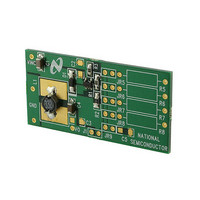
Specifications of LM2831XMF EVAL
LM2831XMFEVAL


Related parts for LM2831XMF EVAL

LM2831XMF EVAL Summary of contents
Page 1
... Additional features in- clude internal soft-start circuitry to reduce inrush current, pulse-by-pulse current limit, thermal shutdown, and output over-voltage protection. Typical Application Circuit © 2006 National Semiconductor Corporation Features n Space Saving SOT23-5 Package n Input voltage range of 3.0V to 5.5V n Output voltage range of 0. ...
Page 2
Connection Diagrams 6-Pin LLP Ordering Information Frequency Order Number Option LM2831XMF LM2831XMFX 1.6MHz LM2831XSD LM2831XSDX LM2831YMF LM2831YMFX 0.55MHz LM2831YSD LM2831YSDX LM2831ZMF LM2831ZMFX 3MHz LM2831ZSD LM2831ZSDX NOPB versions available as well www.national.com 20174801 NSC Package Package Type Drawing SOT23-5 MF05A LLP-6 ...
Page 3
Pin Descriptions 5-Pin SOT23 Pin Name 1 SW Output switch. Connect to the inductor and catch diode. 2 GND Signal and power ground pin. Place the bottom resistor of the feedback network as close as possible to this pin. 3 ...
Page 4
... Absolute Maximum Ratings If Military/Aerospace specified devices are required, please contact the National Semiconductor Sales Office/ Distributors for availability and specifications. VIN FB Voltage EN Voltage SW Voltage ESD Susceptibility Junction Temperature (Note 2) Electrical Characteristics standard type are for T = 25˚C only; limits in boldface type apply over the junction temperature (T J +125˚ ...
Page 5
Electrical Characteristics standard type are for T = 25˚C only; limits in boldface type apply over the junction temperature (T J +125˚C. Minimum and Maximum limits are guaranteed through test, design, or statistical correlation. Typical values represent the most likely ...
Page 6
Typical Performance Characteristics plication circuit shown in Application Information section of this datasheet. T η vs Load "X" Vin = 5V 1.8V & 3.3V η vs Load "Z" Vin = 5V 3.3V & 1.8V Load Regulation ...
Page 7
Typical Performance Characteristics application circuit shown in Application Information section of this datasheet. T specified. (Continued) Load Regulation Vin = 5V 3.3V (All Options) Oscillator Frequency vs Temperature - "Y" Current Limit vs Temperature Vin = 3.3V All ...
Page 8
Typical Performance Characteristics application circuit shown in Application Information section of this datasheet. T specified. (Continued) RDSON vs Temperature (SOT23-5 Package) LM2831Y I (Quiescent Current) Q www.national.com All curves taken at VIN = 5.0V with configuration in typical = 25˚C, ...
Page 9
Typical Performance Characteristics application circuit shown in Application Information section of this datasheet. T specified. (Continued) Line Regulation Vo = 1.8V 500mA Gain vs Frequency (Vin = 5V 1.2V All curves taken at VIN = 5.0V ...
Page 10
Simplified Block Diagram www.national.com FIGURE 1. 10 20174804 ...
Page 11
Applications Information THEORY OF OPERATION The LM2831 is a constant frequency PWM buck regulator IC that delivers a 1.5A load current. The regulator has a preset switching frequency of 550kHz, 1.6MHz, or 3.0MHz. This high frequency allows the LM2831 to ...
Page 12
Design Guide (Continued) FIGURE 3. Inductor Current In general, ) → 0 ∆ OUT If ∆i = 20% of 1.50A, the peak current in the inductor will be L 1.8A. The minimum guaranteed ...
Page 13
Design Guide (Continued) significantly with little detriment to the regulator stability. Like the input capacitor, recommended multilayer ceramic ca- pacitors are X7R or X5R types. CATCH DIODE The catch diode (D1) conducts during the switch off-time. A Schottky diode is ...
Page 14
Calculating Efficiency, and Junction Temperature The complete LM2831 DC/DC converter efficiency can be calculated in the following manner. Or Calculations for determining the most significant power losses are shown below. Other losses totaling less than 2% are not discussed. Power ...
Page 15
... Once this is determined, the maximum ambient temperature allowed for a desired junction temperature can be found. An example of calculating R National Semiconductor LM2831 LLP demonstration board is shown below. The four layer PCB is constructed using FR4 with copper traces. The copper ground plane is on the bottom layer ...
Page 16
LLP Package (Continued) FIGURE 5. 6-Lead LLP PCB Dog Bone Layout www.national.com 20174806 16 ...
Page 17
LM2831X Design Example 1 FIGURE 6. LM2831X (1.6MHz): Vin = 5V 1.2V Part ID U1 1.5A Buck Regulator C1, Input Cap 22µF, 6.3V, X5R C2, Output Cap 2x22µF, 6.3V, X5R D1, Catch Diode 0. ...
Page 18
LM2831X Design Example 2 FIGURE 7. LM2831X (1.6MHz): Vin = 5V 0.6V Part ID U1 C1, Input Cap C2, Output Cap D1, Catch Diode 0. www.national.com Bill of Materials Part Value Manufacturer 1.5A Buck ...
Page 19
LM2831X Design Example 3 FIGURE 8. LM2831X (1.6MHz): Vin = 5V 3.3V Part ID U1 1.5A Buck Regulator C1, Input Cap 22µF, 6.3V, X5R C2, Output Cap 2x22µF, 6.3V, X5R D1, Catch Diode 0. ...
Page 20
LM2831Y Design Example 4 FIGURE 9. LM2831Y (550kHz): Vin = 5V, Vout = 3.3V Part ID U1 1.5A Buck Regulator C1, Input Cap C2, Output Cap D1, Catch Diode 0. www.national.com Bill of Materials Part Value Manufacturer ...
Page 21
LM2831Y Design Example 5 FIGURE 10. LM2831Y (550kHz): Vin = 5V, Vout = 1.2V Part ID U1 1.5A Buck Regulator C1, Input Cap C2, Output Cap 2x22µF, 6.3V, X5R D1, Catch Diode 0. Bill of Materials Part ...
Page 22
LM2831Z Design Example 6 FIGURE 11. LM2831Z (3MHz): Vin = 5V 3.3V Part ID U1 C1, Input Cap C2, Output Cap D1, Catch Diode 0. www.national.com Bill of Materials Part Value Manufacturer 1.5A Buck ...
Page 23
LM2831Z Design Example 7 FIGURE 12. LM2831Z (3MHz): Vin = 5V 1.2V Part ID U1 1.5A Buck Regulator C1, Input Cap 22µF, 6.3V, X5R C2, Output Cap 2x22µF, 6.3V, X5R D1, Catch Diode 0.3V Schottky 1.5A, 30V f ...
Page 24
LM2831X Dual Converters with Delayed Enabled Design Example 8 FIGURE 13. LM2831X (1.6MHz): Vin = 5V 1.2V Part ID U1 C1, C3 Input Cap C2, C4 Output Cap C7 D1, D2 Catch Diode 0.3V L1, L2 ...
Page 25
LM2831X Buck Converter & Voltage Double Circuit with LDO Follower Design Example 9 FIGURE 14. LM2831X (1.6MHz): Vin = 5V 3.3V Part ID Part Value U1 1.5A Buck Regulator U2 200mA LDO C1, Input Cap 22µF, 6.3V, X5R ...
Page 26
Physical Dimensions www.national.com inches (millimeters) unless otherwise noted 5-Lead SOT-23 Package NS Package Number MF05A 6-Lead LLP Package NS Package Number SDE06A 26 ...
Page 27
... BANNED SUBSTANCE COMPLIANCE National Semiconductor follows the provisions of the Product Stewardship Guide for Customers (CSP-9-111C2) and Banned Substances and Materials of Interest Specification (CSP-9-111S2) for regulatory environmental compliance. Details may be found at: www.national.com/quality/green. ...