LM25576EVAL National Semiconductor, LM25576EVAL Datasheet - Page 14
LM25576EVAL
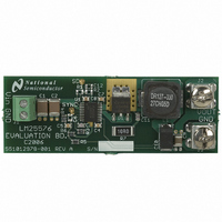
Manufacturer Part Number
LM25576EVAL
Description
BOARD EVALUATION FOR LM25576
Manufacturer
National Semiconductor
Series
PowerWise®, SIMPLE SWITCHER®r
Datasheets
1.LM25576MHNOPB.pdf
(24 pages)
2.LM25576BLDTNOPB.pdf
(4 pages)
3.LM25576EVAL.pdf
(6 pages)
Specifications of LM25576EVAL
Main Purpose
DC/DC, Step Down
Outputs And Type
1, Non-Isolated
Voltage - Output
5V
Current - Output
3A
Voltage - Input
7 ~ 42V
Regulator Topology
Buck
Frequency - Switching
300kHz
Board Type
Fully Populated
Utilized Ic / Part
LM25576
Lead Free Status / RoHS Status
Not applicable / Not applicable
Power - Output
-
Other names
*LM25576EVAL


www.national.com
Application Information
EXTERNAL COMPONENTS
The procedure for calculating the external components is il-
lustrated with the following design example. The Bill of Mate-
rials for this design is listed in Table 1. The circuit shown in
Figure 1 is configured for the following specifications:
•
•
•
•
•
R3 (R
R
frequency applications are smaller but have higher losses.
Operation at 300kHz was selected for this example as a rea-
sonable compromise for both small size and high efficiency.
The value of R
culated as follows:
The nearest standard value of 21kΩ was chosen for R
L1
The inductor value is determined based on the operating fre-
quency, load current, ripple current, and the minimum and
maximum input voltage (V
To keep the circuit in continuous conduction mode (CCM), the
maximum ripple current I
minimum load current, or 0.5Ap-p. Using this value of ripple
current, the value of inductor (L1) is calculated using the fol-
lowing:
This procedure provides a guide to select the value of L1. The
nearest standard value (33µH) will be used. L1 must be rated
for the peak current (I
loading conditions, the peak current occurs at maximum load
current plus maximum ripple. During an overload condition
the peak current is limited to 4.2A nominal (5.1A maximum).
T
V
V
Fs = 300kHz
Minimum load current (for CCM) = 250mA
Maximum load current = 3A
sets the oscillator switching frequency. Generally, higher
OUT
IN
T
)
= 7V to 42V
= 5V
FIGURE 8. Inductor Current Waveform
T
for 300kHz switching frequency can be cal-
PK+
) to prevent saturation. During normal
RIPPLE
IN(min)
should be less than twice the
, V
IN(max)
).
20208710
T
.
14
The selected inductor (see Table 1) has a conservative 6.2
Amp saturation current rating. For this manufacturer, the sat-
uration rating is defined as the current necessary for the
inductance to reduce by 30%, at 20°C.
C3 (C
With the inductor value selected, the value of C3 (C
necessary for the emulation ramp circuit is:
Where L is in Henrys
With L1 selected for 33µH the recommended value for C3 is
330pF.
C9, C10
The output capacitors, C9 and C10, smooth the inductor rip-
ple current and provide a source of charge for transient load-
ing conditions. For this design a 22µF ceramic capacitor and
a 150µF SP organic capacitor were selected. The ceramic
capacitor provides ultra low ESR to reduce the output ripple
voltage and noise spikes, while the SP capacitor provides a
large bulk capacitance in a small volume for transient loading
conditions. An approximation for the output ripple voltage is:
D1
A Schottky type re-circulating diode is required for all
LM25576 applications. Ultra-fast diodes are not recommend-
ed and may result in damage to the IC due to reverse recovery
current transients. The near ideal reverse recovery charac-
teristics and low forward voltage drop are particularly impor-
tant diode characteristics for high input voltage and low output
voltage applications common to the LM25576. The reverse
recovery characteristic determines how long the current
surge lasts each cycle when the buck switch is turned on. The
reverse recovery characteristics of Schottky diodes minimize
the peak instantaneous power in the buck switch occurring
during turn-on each cycle. The resulting switching losses of
the buck switch are significantly reduced when using a Schot-
tky diode. The reverse breakdown rating should be selected
for the maximum V
The forward voltage drop has a significant impact on the con-
version efficiency, especially for applications with a low output
voltage. “Rated” current for diodes vary widely from various
manufacturers. The worst case is to assume a short circuit
load condition. In this case the diode will carry the output cur-
rent almost continuously. For the LM25576 this current can
be as high as 4.2A. Assuming a worst case 1V drop across
the diode, the maximum diode power dissipation can be as
high as 4.2W. For the reference design a 60V Schottky in a
DPAK package was selected.
C1, C2
The regulator supply voltage has a large source impedance
at the switching frequency. Good quality input capacitors are
necessary to limit the ripple voltage at the VIN pin while sup-
plying most of the switch current during the on-time. When the
buck switch turns on, the current into the VIN pin steps to the
lower peak of the inductor current waveform, ramps up to the
peak value, then drops to zero at turn-off. The average current
into VIN during the on-time is the load current. The input ca-
RAMP
)
IN
, plus some safety margin.
C
RAMP
= L x 10
-5
RAMP
)
Related parts for LM25576EVAL
Image
Part Number
Description
Manufacturer
Datasheet
Request
R

Part Number:
Description:
National Semiconductor [8-Bit D/A Converter]
Manufacturer:
National Semiconductor
Datasheet:
Part Number:
Description:
National Semiconductor [Media Coprocessor]
Manufacturer:
National Semiconductor
Datasheet:
Part Number:
Description:
Digitally Controlled Tone and Volume Circuit with Stereo Audio Power Amplifier, Microphone Preamp Stage and National 3D Sound
Manufacturer:
National Semiconductor
Datasheet:
Part Number:
Description:
Digitally Controlled Tone and Volume Circuit with Stereo Audio Power Amplifier, Microphone Preamp Stage and National 3D Sound
Manufacturer:
National Semiconductor
Datasheet:
Part Number:
Description:
AC97 Rev 2 Codec with Sample Rate Conversion and National 3D Sound
Manufacturer:
National Semiconductor
Part Number:
Description:
Manufacturer:
National Semiconductor
Datasheet:
Part Number:
Description:
Manufacturer:
National Semiconductor
Datasheet:
Part Number:
Description:
General Purpose, Low Voltage, Low Power, Rail-to-Rail Output Operational Amplifiers
Manufacturer:
National Semiconductor
Datasheet:
Part Number:
Description:
8-bit 20 MSPS flash A/D converter.
Manufacturer:
National Semiconductor
Datasheet:
Part Number:
Description:
Low Noise Quad Operational Amplifier
Manufacturer:
National Semiconductor
Datasheet:
Part Number:
Description:
Quad Differential Line Receivers
Manufacturer:
National Semiconductor
Datasheet:
Part Number:
Description:
Quad High Speed Trapezoidal? Bus Transceiver
Manufacturer:
National Semiconductor
Datasheet:
Part Number:
Description:
Dual Line Receiver
Manufacturer:
National Semiconductor
Datasheet:
Part Number:
Description:
TTL to 10k ECL Level Translator with Latch
Manufacturer:
National Semiconductor
Datasheet: