LM2653-ADJEVAL National Semiconductor, LM2653-ADJEVAL Datasheet
LM2653-ADJEVAL
Specifications of LM2653-ADJEVAL


Related parts for LM2653-ADJEVAL

LM2653-ADJEVAL Summary of contents
Page 1
... LM2653 battery-powered applications. Synchronous rectification and 75 mΩ internal switches pro- vide up to 97% efficiency. At light loads, the LM2653 enters a low power hysteretic or “sleep” mode to keep the efficiency high. In many applications, the efficiency still exceeds 80 load. A shutdown pin is available to disable the LM2653 and reduce the supply current to 7 µ ...
Page 2
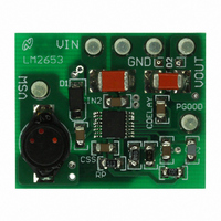
Evaluation Board Design Designation CC2 (compensation) RC (compensation CDELAY RP D2 Typical PC Board Layout: (2X Size) www.national.com (Continued) TABLE 1. Parts List (Bill Of Materials) (Continued) 100pF ceramic capacitor 30kΩ, 5% resistor 1A Schottky diode, Motorola ...
Page 3
... NATIONAL’S PRODUCTS ARE NOT AUTHORIZED FOR USE AS CRITICAL COMPONENTS IN LIFE SUPPORT DEVICES OR SYSTEMS WITHOUT THE EXPRESS WRITTEN APPROVAL OF THE PRESIDENT AND GENERAL COUNSEL OF NATIONAL SEMICONDUCTOR CORPORATION. As used herein: 1. Life support devices or systems are devices or systems which, (a) are intended for surgical implant ...