LM5088MH-2EVAL National Semiconductor, LM5088MH-2EVAL Datasheet - Page 20
LM5088MH-2EVAL
Manufacturer Part Number
LM5088MH-2EVAL
Description
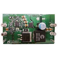
BOARD EVALUATION FOR LM5088MH-2
Manufacturer
National Semiconductor
Series
PowerWise®r
Specifications of LM5088MH-2EVAL
Design Resources
LM(2)5088-1/2 QS Component Calculator
Main Purpose
DC/DC, Step Down
Outputs And Type
1, Non-Isolated
Voltage - Output
5V
Current - Output
7A
Voltage - Input
5.5 ~ 55V
Regulator Topology
Buck
Frequency - Switching
250kHz
Board Type
Fully Populated
Utilized Ic / Part
LM5088
Silicon Manufacturer
National
Silicon Core Number
LM5088
Kit Application Type
Power Management - Voltage Regulator
Application Sub Type
Buck Controller
Kit Contents
Board, Doc
Lead Free Status / RoHS Status
Lead free / RoHS Compliant
Power - Output
-


www.national.com
ERROR AMPLIFIER COMPENSATION
R
characteristics to accomplish a stable voltage loop gain. One
advantage of current mode control is the ability of to close the
loop with only two feedback components R
The voltage loop gain is the product of the modulator gain and
the error amplifier gain. For this example, the modulator can
be treated as an ideal voltage-to-current (transconductance)
converter, The DC modulator gain of the LM5088 can be
modeled as:
DC Gain
The dominant low frequency pole of the modulator is deter-
mined by the load resistance (R
tance (C
For, R
then FP
DC Gain
For the 5V design example the modulator gain vs. frequency
characteristic was measured as shown in Figure 11.
Components R
as a type II compensation configuration. The DC gain of the
amplifier is 80dB which has a pole at low frequency and a zero
at F
set such that it cancels the modulator pole leaving a single
pole response at the crossover frequency of the voltage loop.
A single pole response at the crossover frequency yields a
very stable loop with 90° of phase margin. For the design ex-
ample, a target loop bandwidth (crossover frequency) of 15
kHz was selected. The compensation network zero (F
should be at least an order of magnitude lower than the target
crossover frequency. This constrains the product of R
and C
x R
R
error amp gain. For the design example C
to be 0.015 µF and R
values configure the compensation network zero at 0.6 kHz.
The error amp gain at frequencies greater than F
R
COMP
COMP
COMP
Zero
COMP
COMP
LOAD
, C
, while proportionally decreasing C
/R
= 1/(2
(MOD)
OUT
(MOD)
(MOD)
FB2
COMP
x C
= 5V/7A = 0.714Ω and C
for a desired compensation network zero 1/ (2
). The corner frequency of this pole is:
, which is approximately 3.56 (11dB).
FIGURE 11. Modular Gain Phase
= 550 Hz.
π
= 0.714/ (10 x 10 mΩ) = 7.14 = 17dB
COMP
= R
COMP
and C
x R
LOAD
COMP
) to be less than 1.5 kHz. Increasing
and C
COMP
HF
/ (A x R
x C
configure the error amplifier gain
COMP
was selected to be 18 kΩ. These
COMP
S
)
LOAD
configure the error amplifier
). The error amplifier zero is
OUT
) and the output capaci-
= 500 µF (effective),
COMP
COMP
COMP
, decreases the
was selected
and C
30083934
Zero
COMP
COMP
Zero
π
is
)
.
20
The overall voltage loop gain can be predicted as the sum (in
dB) of the modulator gain and the error amp gain. If a network
analyzer is available, the modulator gain can be measured
and the error amplifier gain can be configured for the desired
loop transfer function. If a network analyzer is not available,
the error amplifier compensation components can be de-
signed with the suggested guidelines. Step load transient
tests can be performed to verify performance. The step load
goal is minimum overshoot with a damped response. C
be added to the compensation network to decrease noise
susceptibility of the error amplifier. The value of C
sufficiently small since the addition of this capacitor adds a
pole in the error amplifier transfer function. A good approxi-
mation of the location of the pole added by C
F
coupling of any switching noise into the modulator. The value
of C
Zero
HF
x C
FIGURE 12. Error Amplifier Gain and Phase
was selected as 100 pF for this design example.
FIGURE 13. Overall Loop Gain and Phase
COMP
/ C
HF
.Using C
HF
is recommended to minimize
HF
HF
30083935
30083936
is F
must be
HF
P2
can
=
Related parts for LM5088MH-2EVAL
Image
Part Number
Description
Manufacturer
Datasheet
Request
R

Part Number:
Description:
IC BUCK ADJ 10A TSSOP16EP
Manufacturer:
National Semiconductor
Datasheet:
Part Number:
Description:
IC BUCK ADJ 10A TSSOP16EP
Manufacturer:
National Semiconductor
Datasheet:

Part Number:
Description:
LM5088MH-1 EVAL BOARD
Manufacturer:
National Semiconductor
Datasheet:
Part Number:
Description:
BOARD EVALUATION FOR LM5088MH-1
Manufacturer:
National Semiconductor
Datasheet:

Part Number:
Description:
Wide Input Range Non-Synchronous Buck Controller
Manufacturer:
NSC [National Semiconductor]
Datasheet:
Part Number:
Description:
National Semiconductor [8-Bit D/A Converter]
Manufacturer:
National Semiconductor
Datasheet:
Part Number:
Description:
National Semiconductor [Media Coprocessor]
Manufacturer:
National Semiconductor
Datasheet:
Part Number:
Description:
Digitally Controlled Tone and Volume Circuit with Stereo Audio Power Amplifier, Microphone Preamp Stage and National 3D Sound
Manufacturer:
National Semiconductor
Datasheet:
Part Number:
Description:
Digitally Controlled Tone and Volume Circuit with Stereo Audio Power Amplifier, Microphone Preamp Stage and National 3D Sound
Manufacturer:
National Semiconductor
Datasheet:
Part Number:
Description:
AC97 Rev 2 Codec with Sample Rate Conversion and National 3D Sound
Manufacturer:
National Semiconductor
Part Number:
Description:
Manufacturer:
National Semiconductor
Datasheet:
Part Number:
Description:
Manufacturer:
National Semiconductor
Datasheet:
Part Number:
Description:
General Purpose, Low Voltage, Low Power, Rail-to-Rail Output Operational Amplifiers
Manufacturer:
National Semiconductor
Datasheet:
Part Number:
Description:
8-bit 20 MSPS flash A/D converter.
Manufacturer:
National Semiconductor
Datasheet: