LM2595ATPBCKGEVB ON Semiconductor, LM2595ATPBCKGEVB Datasheet - Page 3
LM2595ATPBCKGEVB
Manufacturer Part Number
LM2595ATPBCKGEVB
Description
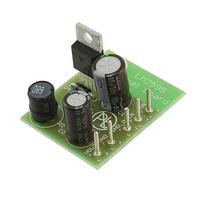
EVAL BOARD FOR LM2595ATPBCKG
Manufacturer
ON Semiconductor
Specifications of LM2595ATPBCKGEVB
Design Resources
LM2595ATPBCKGEVB BOM LM2595ATPBCKGEVB Gerber Files LM2595ATPBCKGEVB Schematic
Main Purpose
DC/DC, Step Down
Outputs And Type
1, Non-Isolated
Voltage - Output
5V
Current - Output
1A
Voltage - Input
4.5 ~ 40 V
Regulator Topology
Buck
Frequency - Switching
150kHz
Board Type
Fully Populated
Utilized Ic / Part
LM2595
Lead Free Status / RoHS Status
Lead free / RoHS Compliant
Power - Output
-
Lead Free Status / Rohs Status
Lead free / RoHS Compliant
For Use With/related Products
LM2595ATPBCKG
Other names
LM2595ATPBCKGEVBOS


PIN FUNCTION DESCRIPTION
OPERATING RATINGS
specific performance limits. For guaranteed specifications and test conditions, see the Electrical Characteristics.)
Pin
Operating Junction Temperature Range
Supply Voltage
1
2
3
4
5
Feedback
ON/OFF
Symbol
Output
GND
V
in
This is the emitter of the internal switch. The saturation voltage V
kept in mind that the PCB area connected to this pin should be kept to a minimum in order to minimize coupling to
sensitive circuitry.
This pin is the positive input supply for the LM2595 step−down switching regulator. In order to minimize voltage transi-
ents and to supply the switching currents needed by the regulator, a suitable input bypass capacitor must be present
(C
Circuit ground pin. See the information about the printed circuit board layout.
This pin is the direct input of the error amplifier and the resistor network R2, R1 is connected externally to allow pro-
gramming of the output voltage.
It allows the switching regulator circuit to be shut down using logic level signals, thus dropping the total input supply
current to approximately 50 mA. The threshold voltage is typically 1.6 V. Applying a voltage above this value (up to
+V
will be in the “on” condition.
in
in
) shuts the regulator off. If the voltage applied to this pin is lower than 1.6 V or if this pin is left open, the regulator
in Figure 1).
(Operating Ratings indicate conditions for which the device is intended to be functional, but do not guarantee
Rating
http://onsemi.com
Description (Refer to Figure 1)
3
sat
of this output switch is typically 1.0 V. It should be
Symbol
V
T
in
J
−40 to +125
4.5 to 40
Value
Unit
°C
V
Related parts for LM2595ATPBCKGEVB
Image
Part Number
Description
Manufacturer
Datasheet
Request
R

Part Number:
Description:
ON Semiconductor [VOLTAGE REGULATOR]
Manufacturer:
ON Semiconductor
Datasheet:
Part Number:
Description:
357-036-542-201 CARDEDGE 36POS DL .156 BLK LOPRO
Manufacturer:
ON Semiconductor
Datasheet:
Part Number:
Description:
357-036-542-201 CARDEDGE 36POS DL .156 BLK LOPRO
Manufacturer:
ON Semiconductor
Datasheet:
Part Number:
Description:
357-036-542-201 CARDEDGE 36POS DL .156 BLK LOPRO
Manufacturer:
ON Semiconductor
Datasheet:
Part Number:
Description:
357-036-542-201 CARDEDGE 36POS DL .156 BLK LOPRO
Manufacturer:
ON Semiconductor
Datasheet:
Part Number:
Description:
357-036-542-201 CARDEDGE 36POS DL .156 BLK LOPRO
Manufacturer:
ON Semiconductor
Datasheet:
Part Number:
Description:
357-036-542-201 CARDEDGE 36POS DL .156 BLK LOPRO
Manufacturer:
ON Semiconductor
Datasheet:
Part Number:
Description:
357-036-542-201 CARDEDGE 36POS DL .156 BLK LOPRO
Manufacturer:
ON Semiconductor
Datasheet:
Part Number:
Description:
357-036-542-201 CARDEDGE 36POS DL .156 BLK LOPRO
Manufacturer:
ON Semiconductor
Datasheet:
Part Number:
Description:
357-036-542-201 CARDEDGE 36POS DL .156 BLK LOPRO
Manufacturer:
ON Semiconductor
Datasheet:
Part Number:
Description:
357-036-542-201 CARDEDGE 36POS DL .156 BLK LOPRO
Manufacturer:
ON Semiconductor
Datasheet:
Part Number:
Description:
Manufacturer:
ON Semiconductor
Datasheet:
Part Number:
Description:
Manufacturer:
ON Semiconductor
Datasheet:
Part Number:
Description:
Manufacturer:
ON Semiconductor
Datasheet: