MCP4725DM-PTPLS Microchip Technology, MCP4725DM-PTPLS Datasheet - Page 12
MCP4725DM-PTPLS
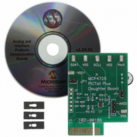
Manufacturer Part Number
MCP4725DM-PTPLS
Description
BOARD DAUGHTER PICTAIL MCP4725
Manufacturer
Microchip Technology
Specifications of MCP4725DM-PTPLS
Number Of Dac's
1
Number Of Bits
12
Outputs And Type
1, Single Ended
Sampling Rate (per Second)
100k ~ 3.4M
Data Interface
I²C
Settling Time
6µs
Dac Type
Voltage
Voltage Supply Source
Single
Operating Temperature
-40°C ~ 125°C
Utilized Ic / Part
MCP4725
Silicon Manufacturer
Microchip
Application Sub Type
DAC
Kit Application Type
Data Converter
Silicon Core Number
MCP4725
Silicon Family Name
PICtail
Lead Free Status / RoHS Status
Lead free / RoHS Compliant
Available stocks
Company
Part Number
Manufacturer
Quantity
Price
Company:

Part Number:
MCP4725DM-PTPLS
Manufacturer:
Microchip Technology
Quantity:
135


MCP4725 PICtail™ Plus Daughter Board User’s Guide
DS51722A-page 8
1.3.2.2
Figure 1-5 shows the flow chart of the firmware. Once the MCU firmware is pro-
grammed, the user can observe the following events:
1. V
2. Audible sounds (Buzzer) if JP4 is connected.
3. I
1.3.3
The MCU sends write commands for EEPROM and DAC input register.
The MCU writes EEPROM only once, but writes continuously the DAC input register.
The EEPROM is written for the V
ously written for the V
“FFFh” with 1 LSB increment. When it reaches “FFFh”, resets to “000h” and repeats the
writing from “000h” to “FFFh” with 1 LSB again.
The user can observe the V
oscilloscope. Figure 1-7 shows the I
output waveform.
The DAC input register is written with fast mode write command which does not affect
the EEPROM. The user can confirm the data written in EEPROM (V
disconnecting the MCP4725 PICtail™ Plus Daughter Board from the Explorer 16
Development Board. When the board is first powered, the MCP4725 device loads the
EEPROM data to the DAC input register by itself and then outputs an analog voltage
determined by the EEPROM data.
1.3.4
The MCP4725 PICtail™ Plus Daughter Board includes a buzzer. This buzzer is directly
connected to the V
buzzer sounds also can be adjusted by VR1.
waveform.
Figure 1-6 and Figure 1-7.
2
OUT
C data communication (SDA and SCL) waveform over the I
changes as the MCU rewrites the DAC codes. See Figure 1-6 for the V
DAC Output (V
Audible Buzzer
FIRMWARE FLOW CHART FOR THE MCP4725 DAUGHTER BOARD
OUT
OUT
. The user can disable the buzzer by disconnecting JP4. The
to be ramp: The DAC input code is written from “000h” to
OUT
OUT
)
at the V
OUT
2
C clock (SCL) and data (SDA) signals, and DAC
= V
OUT
DD
/2, and the DAC input register is continu-
test pin using a digital voltmeter or
© 2008 Microchip Technology Inc.
2
C bus line. See
OUT
= V
DD
/2) by
OUT
Related parts for MCP4725DM-PTPLS
Image
Part Number
Description
Manufacturer
Datasheet
Request
R

Part Number:
Description:
Manufacturer:
Microchip Technology Inc.
Datasheet:
Part Number:
Description:
Manufacturer:
Microchip Technology Inc.
Datasheet:
Part Number:
Description:
Manufacturer:
Microchip Technology Inc.
Datasheet:
Part Number:
Description:
Manufacturer:
Microchip Technology Inc.
Datasheet:
Part Number:
Description:
Manufacturer:
Microchip Technology Inc.
Datasheet:
Part Number:
Description:
Manufacturer:
Microchip Technology Inc.
Datasheet:
Part Number:
Description:
Manufacturer:
Microchip Technology Inc.
Datasheet:
Part Number:
Description:
Manufacturer:
Microchip Technology Inc.
Datasheet: