CDB4353 Cirrus Logic Inc, CDB4353 Datasheet
CDB4353
Specifications of CDB4353
CDB-4353


Related parts for CDB4353


CDB4353 Summary of contents
Page 1
... The CDB4353 is controlled by switches to select the digital signal source and configuration options for the CS4353. Current sense resistors allow for easy power calculations during system development. ...
Page 2
... TABLE OF CONTENTS 1. CDB4353 SYSTEM OVERVIEW ............................................................................................................ 4 2. CS4353 DIGITAL-TO-ANALOG CONVERTER ..................................................................................... 4 3. CS8416 DIGITAL AUDIO RECEIVER .................................................................................................... 4 4. INPUT FOR CLOCKS AND DATA ......................................................................................................... 4 5. POWER SUPPLY CIRCUITRY ............................................................................................................... 5 6. GROUNDING AND POWER SUPPLY DECOUPLING .......................................................................... 5 7. HARDWARE CONTROL ........................................................................................................................ 5 8. CS8416 AND CS4353 RESET ............................................................................................................... 5 9. ANALOG OUTPUT FILTERING ............................................................................................................. 5 10 ...
Page 3
... LIST OF TABLES Table 1. Switch S1 Quick Setup .................................................................................................................. 5 Table 2. System Connections .................................................................................................................... 6 Table 3. CDB4353 Jumper Settings ............................................................................................................ 6 Table 4. CDB4353 Switch Settings ............................................................................................................. 6 DS803DB2 CDB4353 3 ...
Page 4
... CDB4353 SYSTEM OVERVIEW The CDB4353 evaluation board is an excellent means of quickly evaluating the CS4353. The CS8416 digital audio interface receiver provides an easy interface to digital audio signal sources, including the majority of digital audio test equipment. The evaluation board also allows the user to supply external PCM clocks and data through two sep- arate header options for system development ...
Page 5
... CS4353 as possible. 7. HARDWARE CONTROL The CDB4353 is controlled through settings on switch S1. This allows for configuration of the board without a PC. Switch S1 can toggle settings for CS8416 MCLK speed, CS8416 and CS4353 PCM data format, clock and data source for the board, and the Hardware Mode configuration of the CS4353. ...
Page 6
... When shunt is removed, the voltage can be measured *shunted across a fixed resistance to determine current. When shunt is removed, the voltage can be measured *shunted across a fixed resistance to determine current. *EXTERNAL POR *shunted not shunted Table 3. CDB4353 Jumper Settings POSITION CS8416 must be reset if switch S1 position Table 4. CDB4353 Switch Settings CDB4353 below ...
Page 7
... PLOTS Test conditions (unless otherwise specified 25°C; VCP = 3.3 V; AGND = DGND =CPGND = 0 V; OPT1 S/PDIF input source; PCM data Left-Justified format 997 Hz sine wave at 0 dBFS; dB values relative to 2 kHz. CDB4353 revision A3 with CS4353 revision B1 used. +0 -10 -20 -30 -40 -50 - -70 r -80 ...
Page 8
... Figure 10. 48 kHz, Impulse Response +0 -10 -20 -30 -40 -50 - -70 r -80 A -90 -100 -110 -120 -130 -140 -150 2k 5k 10k 20k 20 50 Figure 12. FFT (96 kHz, -60 dB) CDB4353 100 200 500 10k 20k Hz 1m 1.5m 2m 2.5m sec 100 200 500 10k 20k Hz DS803DB2 3m ...
Page 9
... Figure 14. FFT (96 kHz Out-of-Band, No Input) +0 -10 -20 -30 - -60 A -70 -80 -90 -100 -110 2k 5k 10k 20k -120 Figure 16. 96 kHz, THD+N vs. Level + -40 - Figure 18. 96 kHz, Frequency Response CDB4353 20k 40k 60k 80k 100k Hz -100 -80 -60 -40 -20 dBFS 100 200 500 10k Hz 120k +0 20k 9 ...
Page 10
... Figure 22. FFT (192 kHz, -60 dB) +0 -10 -20 -30 -40 -50 - -70 r -80 A -90 -100 -110 -120 -130 -140 -150 2k 5k 10k 20k Figure 24. FFT (192 kHz Out-of-Band, No Input) CDB4353 500u 1m sec 100 200 500 10k Hz 20k 40k 60k 80k 100k Hz DS803DB2 1.5m 20k 120k ...
Page 11
... Figure 26. 192 kHz, THD+N vs. Level + -40 -20 +0 Figure 28. 192 kHz, Frequency Response 3 2.5 2 1.5 1 500m 0 V -500m -1 -1 10k 20k Figure 30. 192 kHz, Impulse Response CDB4353 -100 -80 -60 -40 -20 dBFS 100 200 500 10k Hz 200u 400u 600u sec +0 20k 11 ...
Page 12
AND LAYOUT +3.3V Power (Optional separate VL) Figure 33 PCM HEADER PCM Clocks/Data PCM Input Figure 33 PCM Mux and Level Figure 33 Optical PCM Clocks/Data S/PDIF Input CS8416 S/PDIF CS8416 serial port format Receiver Coaxial Figure 32 S/PDIF ...
Page 13
Figure 32. CS8416 and CS4353 ...
Page 14
Figure 33. HW Configuration, PCM Header, and Power ...
Page 15
Figure 34. Silkscreen Top ...
Page 16
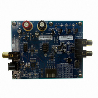
Figure 35. Top Side ...
Page 17
Figure 36. Bottom Side ...
Page 18
... TORNEYS’ FEES AND COSTS, THAT MAY RESULT FROM OR ARISE IN CONNECTION WITH THESE USES. Cirrus Logic, Cirrus, and the Cirrus Logic logo designs are trademarks of Cirrus Logic, Inc. All other brand and product names in this document may be trademarks or service marks of their respective owners. 18 Changes page 1 and Figure 31. page 1. Plots. Figure 33. www.cirrus.com. CDB4353 DS803DB2 ...