CDB4351 Cirrus Logic Inc, CDB4351 Datasheet
CDB4351
Specifications of CDB4351


Related parts for CDB4351


CDB4351 Summary of contents
Page 1
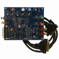
... Digital Audio Interface http://www.cirrus.com Description The CDB4351 evaluation board is an excellent means for quickly evaluating the CS4351 24-bit, high perfor- mance stereo D/A converter. Evaluation requires an analog signal analyzer, a digital signal source for controlling the CS4351 (stand alone operation is also available) and a power supply ...
Page 2
... LIST OF FIGURES Figure 1. System Block Diagram and Signal Flow . . . . . . . . . . . . . . . . . . . . . . . . . . . . . . . . . . . 6 Figure 2. CS4351 . . . . . . . . . . . . . . . . . . . . . . . . . . . . . . . . . . . . . . . . . . . . . . . . . . . . . . . . . . . . . . 7 Figure 3. Analog Outputs . . . . . . . . . . . . . . . . . . . . . . . . . . . . . . . . . . . . . . . . . . . . . . . . . . . . . . . 8 Figure 4. PCM Input Headers . . . . . . . . . . . . . . . . . . . . . . . . . . . . . . . . . . . . . . . . . . . . . . . . . . . . 9 Figure 5. CS8416 S/PDIF Input . . . . . . . . . . . . . . . . . . . . . . . . . . . . . . . . . . . . . . . . . . . . . . . . . . 10 Figure 6. Control Port Interface . . . . . . . . . . . . . . . . . . . . . . . . . . . . . . . . . . . . . . . . . . . . . . . . . 11 Figure 7. Power Supply Connections . . . . . . . . . . . . . . . . . . . . . . . . . . . . . . . . . . . . . . . . . . . . 12 Figure 8. Silkscreen Top Figure 9. Top Side . . . . . . . . . . . . . . . . . . . . . . . . . . . . . . . . . . . . . . . . . . . . . . . . . . . . . . . . . . . . 14 Figure 10. Bottom Side . . . . . . . . . . . . . . . . . . . . . . . . . . . . . . . . . . . . . . . . . . . . . . . . . . . . . . . . 15 2 CDB4351 DS566DB3 ...
Page 3
... The evaluation board also allows the user to supply external PCM clocks and data through a header for system development. The CDB4351 schematic has been partitioned into 6 schematics shown in Figures 2 through 7. Each partitioned schematic is represented in the system diagram shown in Figure 1. Notice that the system diagram also includes the interconnections between the partitioned schematics ...
Page 4
... ANALOG OUTPUT FILTERING The analog output on the CDB4351 has been designed according to the CS4351 datasheet. This output circuit includes an AC coupling cap, the FET mute circuit, and a single-pole R and C. An additional load resistance of 5.1 kΩ can be jumpered in (J15 and J24) to test the CS4351’s load driving capability ...
Page 5
... S * SHUNTED *OPEN *SHUNTED OPEN Table 2. CDB4351 Jumper Settings CDB4351 FUNCTION SELECTED Voltage source binding post Voltage source regulator Voltage source is VD binding post Voltage source is +3.3 V regulator Voltage source is VL binding post Voltage source is +3.3 V regulator Voltage source is VA binding post Voltage source is +3 ...
Page 6
... CDB4351 DS566DB3 ...
Page 7
... DS566DB3 CDB4351 7 ...
Page 8
... CDB4351 DS566DB3 ...
Page 9
... DS566DB3 CDB4351 9 ...
Page 10
... CDB4351 DS566DB3 ...
Page 11
... DS566DB3 CDB4351 11 ...
Page 12
... CDB4351 DS566DB3 ...
Page 13
... DS566DB3 Figure 8. Silkscreen Top CDB4351 13 ...
Page 14
... Figure 9. Top Side CDB4351 DS566DB3 ...
Page 15
... DS566DB3 Figure 10. Bottom Side CDB4351 15 ...
Page 16
... C Patent Rights to use those components in a standard I 16 REVISION HISTORY Initial Release Updated figures 2 and 5 (C48 and R65) Updated schematic and layout figures to match rev B of the PCB 2 C Components of Cirrus Logic, Inc., or one of its sublicensed Associated Companies 2 C system. CDB4351 Changes DS566DB3 ...