CDB4352 Cirrus Logic Inc, CDB4352 Datasheet - Page 2
CDB4352
Manufacturer Part Number
CDB4352
Description
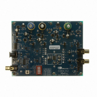
BOARD EVAL FOR CS4352 DAC
Manufacturer
Cirrus Logic Inc
Series
Popguard®r
Specifications of CDB4352
Number Of Dac's
2
Number Of Bits
24
Outputs And Type
2, Single Ended
Sampling Rate (per Second)
192k
Data Interface
Serial
Dac Type
Voltage
Voltage Supply Source
Analog and Digital
Operating Temperature
-40°C ~ 85°C
Utilized Ic / Part
CS4352
Description/function
Audio D/A
Operating Supply Voltage
3.3 V
Product
Audio Modules
For Use With/related Products
CS4352
Lead Free Status / RoHS Status
Contains lead / RoHS non-compliant
Lead Free Status / RoHS Status
Lead free / RoHS Compliant, Contains lead / RoHS non-compliant
Other names
598-1518


2
TABLE OF CONTENTS
LIST OF FIGURES
LIST OF TABLES
1. PIN DESCRIPTIONS ............................................................................................................................. 3
2. CHARACTERISTICS AND SPECIFICATIONS ...................................................................................... 4
3. TYPICAL CONNECTION DIAGRAM ................................................................................................... 10
4. APPLICATIONS ................................................................................................................................... 11
5. DIGITAL FILTER RESPONSE PLOTS
6. PARAMETER DEFINITIONS ................................................................................................................ 18
7. PACKAGE DIMENSIONS ................................................................................................................... 19
8. ORDERING INFORMATION ............................................................................................................... 20
9. REVISION HISTORY ............................................................................................................................ 20
Figure 1.Serial Input Timing ........................................................................................................................ 8
Figure 2.Typical Connection Diagram ....................................................................................................... 10
Figure 3.I²S, up to 24-Bit Data .................................................................................................................. 12
Figure 4.Right-Justified Data ..................................................................................................................... 12
Figure 5.Left-Justified up to 24-Bit Data .................................................................................................... 12
Figure 6.De-Emphasis Curve .................................................................................................................... 13
Figure 7.Single-Speed Stopband Rejection .............................................................................................. 16
Figure 8.Single-Speed Transition Band .................................................................................................... 16
Figure 9.Single-Speed Transition Band (detail) ........................................................................................ 16
Figure 10.Single-Speed Passband Ripple ................................................................................................ 16
Figure 11.Double-Speed Stopband Rejection ........................................................................................... 16
Figure 12.Double-Speed Transition Band ................................................................................................. 16
Figure 13.Double-Speed Transition Band (detail) ..................................................................................... 17
Figure 14.Double-Speed Passband Ripple ............................................................................................... 17
Figure 15.Quad-Speed Stopband Rejection ............................................................................................. 17
Figure 16.Quad-Speed Transition Band ................................................................................................... 17
Figure 17.Quad-Speed Transition Band (detail) ....................................................................................... 17
Figure 18.Quad-Speed Passband Ripple ................................................................................................. 17
Table 1. CS4352 Auto-Detect ................................................................................................................... 11
Table 2. Single-Speed Mode Standard Frequencies ................................................................................ 11
Table 3. Double-Speed Mode Standard Frequencies ............................................................................... 11
Table 4. Quad-Speed Mode Standard Frequencies ................................................................................. 11
Table 5. Digital Interface Format ............................................................................................................... 12
RECOMMENDED OPERATING CONDITIONS .................................................................................... 4
ABSOLUTE MAXIMUM RATINGS ........................................................................................................ 4
DAC ANALOG CHARACTERISTICS - COMMERCIAL (-CZZ) ............................................................. 5
DAC ANALOG CHARACTERISTICS - AUTOMOTIVE (-DZZ) .............................................................. 6
COMBINED INTERPOLATION & ON-CHIP ANALOG FILTER RESPONSE ........................................ 7
SWITCHING SPECIFICATIONS - SERIAL AUDIO INTERFACE
DIGITAL CHARACTERISTICS .............................................................................................................. 9
POWER AND THERMAL CHARACTERISTICS ................................................................................... 9
4.6.1 Capacitor Placement ............................................................................................................. 13
4.7.1 Power-Up .............................................................................................................................. 14
4.7.2 Power-Down .......................................................................................................................... 14
4.7.3 Discharge Time ..................................................................................................................... 14
......................................................................................... 16
................................................... 8
CS4352
DS684F2
Related parts for CDB4352
Image
Part Number
Description
Manufacturer
Datasheet
Request
R

Part Number:
Description:
Development Kit
Manufacturer:
Cirrus Logic Inc
Datasheet:
Part Number:
Description:
Development Kit
Manufacturer:
Cirrus Logic Inc
Datasheet:


Part Number:
Description:
High-efficiency PFC + Fluorescent Lamp Driver Reference Design
Manufacturer:
Cirrus Logic Inc
Datasheet:
Part Number:
Description:
Development Kit
Manufacturer:
Cirrus Logic Inc
Datasheet:
Part Number:
Description:
Development Kit
Manufacturer:
Cirrus Logic Inc
Datasheet:

Part Number:
Description:
Development Kit
Manufacturer:
Cirrus Logic Inc
Datasheet:
Part Number:
Description:
Development Kit
Manufacturer:
Cirrus Logic Inc
Datasheet:
Part Number:
Description:
Development Kit
Manufacturer:
Cirrus Logic Inc
Datasheet:
Part Number:
Description:
Development Kit
Manufacturer:
Cirrus Logic Inc
Datasheet:

Part Number:
Description:
EVALUATION BOARD FOR CS8427
Manufacturer:
Cirrus Logic Inc
Datasheet:

Part Number:
Description:
BOARD EVAL FOR CS8416 RCVR
Manufacturer:
Cirrus Logic Inc
Datasheet:

Part Number:
Description:
EVALUATION BOARD FOR CS8420
Manufacturer:
Cirrus Logic Inc
Datasheet:

Part Number:
Description:
KIT DEVELOPMENT EP9315 ARM9
Manufacturer:
Cirrus Logic Inc
Datasheet:

Part Number:
Description:
KIT DEVELOPMENT EP9302 ARM9
Manufacturer:
Cirrus Logic Inc
Datasheet: