DK86065-2 Fujitsu Semiconductor America Inc, DK86065-2 Datasheet - Page 10
DK86065-2
Manufacturer Part Number
DK86065-2
Description
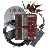
KIT EVAL 16BIT DAC FOR MB86065
Manufacturer
Fujitsu Semiconductor America Inc
Specifications of DK86065-2
Number Of Dac's
1
Number Of Bits
14
Outputs And Type
1, Differential
Sampling Rate (per Second)
1G
Data Interface
Serial
Dac Type
Current
Voltage Supply Source
Analog and Digital
Operating Temperature
-40°C ~ 85°C
Utilized Ic / Part
MB86065
For Use With
865-1111 - DAC DK FPGA ADAPTER BOARD865-1012 - KIT DEV DUAL 14BIT MB86064 SMA
Lead Free Status / RoHS Status
Lead free / RoHS Compliant
Other names
865-1011


Connections to the loop clock are via pins LPCLK_IN and LPCLK_OUT. The loop clock delay is
programmed through register SYSTEM CLOCK DELAYS, loop_clk_dly. See Table 8.
With the DAC Core Clock Delays set to their recommended values (0x00), monitoring the analog
output for a valid signal while adjusting the Clock Output and Loop Clock delays enables a diagram
of valid & invalid data latching points to be produced. An example is illustrated in Figure 4.
This example used an Altera Stratix FPGA evaluation platform driving a Fujitsu development kit at
800MSa/s. Another circuit implementation would exhibit different absolute timings but similar relative
adjustments.
Having evaluated a prototype design and final loop clock delay settings chosen, the real benefit of
using the loop clock facility is in maintaining valid clock-to-data timing at these settings. Figure 5
illustrates this in operation by using excessive variation in supply voltages to emulate both fast and
slow FPGA and DAC components being used together in production.
Page 10 of 56
Disclaimer : The contents of this document are subject to change without notice. Customers are advised to consult with FUJITSU sales representatives before
DAC CORE
DELAYS
CLOCK
[0x1B2]
loop_clk_dly
00
ordering.The information and circuit diagrams in this document are presented “as is”, no license is granted by implication or otherwise.
Table 8: DAC Core Register: SYSTEM CLOCK DELAYS [0x1C1] (Part 4 of 4)
Label
-1.5ns
It is important not to adjust both delays simultaneously else they will counteract each other.
Either the Clock Output delay or the Loop Clock delay, or both, should be zero.
Figure 4 Finding Valid Data Eyes Using Loop Clock
Retard bits [7:4] or [3:0] (0 - 1.5ns)
11
0
1
:
Production
Reg Bits
10
0
1
:
9
0
1
:
SYSTEM CLOCK DELAYS Register [0x1C1]
8
0
1
:
Minimum (default)
Maximum
0
Copyright © 2004-2007 Fujitsu Microelectronics Europe GmbH
MB86065 14-bit 1+GSa/s DAC
(0 - 1.5ns, 100ps steps)
Advance bits [11:8] (0 - 1.5ns)
Loop Clock Delay
September 2007 Version 1.01
FME/MS/DAC80S/DS/5344
+1.5ns
Related parts for DK86065-2
Image
Part Number
Description
Manufacturer
Datasheet
Request
R

Part Number:
Description:
IC POWER SUPPLY MONITOR 8SOP
Manufacturer:
Fujitsu Semiconductor America Inc
Datasheet:
Part Number:
Description:
IC POWER SUPPLY MONITOR 8SOP
Manufacturer:
Fujitsu Semiconductor America Inc
Datasheet:

Part Number:
Description:
IC MCU 60K FLASH 2KB RAM 52LQFP
Manufacturer:
Fujitsu Semiconductor America Inc
Datasheet:

Part Number:
Description:
IC MCU 32BIT 256KB FLASH 120LQFP
Manufacturer:
Fujitsu Semiconductor America Inc
Datasheet:
Part Number:
Description:
IC CTLR TOUCH SENSOR 12CH 30SSOP
Manufacturer:
Fujitsu Semiconductor America Inc
Datasheet:

Part Number:
Description:
IC CTLR TOUCH SENSOR 12CH 40QFN
Manufacturer:
Fujitsu Semiconductor America Inc
Datasheet:
Part Number:
Description:
SYNTHESIZER PLL DUAL INP 20SSOP
Manufacturer:
Fujitsu Semiconductor America Inc
Datasheet:

Part Number:
Description:
SYNTHESZR PLL 1.1GHZ DUAL 16SSOP
Manufacturer:
Fujitsu Semiconductor America Inc
Datasheet:

Part Number:
Description:
IC SSCG EMI RED 8-SOIC
Manufacturer:
Fujitsu Semiconductor America Inc
Datasheet:

Part Number:
Description:
IC SSCG EMI RED 8-TSSOP
Manufacturer:
Fujitsu Semiconductor America Inc
Datasheet:

Part Number:
Description:
IC SSCG EMI RED 8-SOP
Manufacturer:
Fujitsu Semiconductor America Inc
Datasheet:

Part Number:
Description:
SYNTHESIZER PLL 2.5GHZ 16SSOP
Manufacturer:
Fujitsu Semiconductor America Inc
Datasheet:
Part Number:
Description:
SYNTHESIZER PLL 1.2GHZ 16SSOP
Manufacturer:
Fujitsu Semiconductor America Inc
Datasheet:

Part Number:
Description:
SYNTHESIZER PLL 2.5GHZ 16BCC
Manufacturer:
Fujitsu Semiconductor America Inc
Datasheet:

Part Number:
Description:
IC SSCG EMI RED 8-SOP
Manufacturer:
Fujitsu Semiconductor America Inc
Datasheet: