EVAL-AD5821EBZ Analog Devices Inc, EVAL-AD5821EBZ Datasheet - Page 3
EVAL-AD5821EBZ
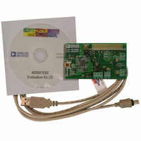
Manufacturer Part Number
EVAL-AD5821EBZ
Description
BOARD EVALUATION FOR AD5821
Manufacturer
Analog Devices Inc
Datasheet
1.AD5821ABCBZ-REEL7.pdf
(16 pages)
Specifications of EVAL-AD5821EBZ
Number Of Dac's
1
Number Of Bits
10
Outputs And Type
1, Single Ended
Sampling Rate (per Second)
400k
Data Interface
I²C
Settling Time
250µs
Dac Type
Current
Voltage Supply Source
Single
Operating Temperature
-30°C ~ 80°C
Utilized Ic / Part
AD5821
Lead Free Status / RoHS Status
Lead free / RoHS Compliant


SPECIFICATIONS
V
unless otherwise noted.
Table 1.
Parameter
DC PERFORMANCE
OUTPUT CHARACTERISTICS
LOGIC INPUTS (XSHUTDOWN)
LOGIC INPUTS (SCL, SDA)
POWER REQUIREMENTS
1
2
3
4
5
6
7
Temperature range is as follows: B Version = −30°C to +85°C.
See the
Linearity is tested using a reduced code range: Code 32 to Code 1023.
To achieve near zero output current, use the power-down feature.
Guaranteed by design and characterization; not production tested. XSHUTDOWN is active low. SDA and SCL pull-up resistors are tied to 1.8 V.
Input filtering on both the SCL and the SDA inputs suppresses noise spikes that are less than 50 ns.
XSHUTDOWN is active low.
DD
Minimum Sink Current
Maximum Sink Current
Output Current During XSHUTDOWN
Output Compliance
Output Compliance
Power-Up Time
Input Current
Input Low Voltage, V
Input High Voltage, V
Pin Capacitance
Input Low Voltage, V
Input High Voltage, V
Input Low Voltage, V
Input High Voltage, V
Input Leakage Current, I
Input Hysteresis, V
Digital Input Capacitance, C
Glitch Rejection
V
I
V
I
Resolution
Relative Accuracy
Differential Nonlinearity
Zero-Code Error
Offset Error @ Code 16
Gain Error
Offset Error Drift
Gain Error Drift
DD
DD
DD
DD
= 2.7 V to 5.5 V, AGND = DGND = 0 V, load resistance R
(Normal Mode)
(Power-Down Mode)
= 2.7 V to 3.6 V
Terminology
2
2, 5
6
2, 4
section.
4, 5
2
HYST
5
5
INL
INL
INL
INH
INH
INH
2
4
5
IN
7
2, 3
5
IN
Min
0
0.6
0.48
1.3
−0.3
1.26
−0.3
1.4
0.05 V
2.7
DD
B Version
Typ
10
±1.5
1
0.5
10
±0.2
3
120
80
20
3
6
2.5
0.5
1
Max
±4
±1
5
±0.6
±0.5
V
V
±1
0.54
+0.54
V
+0.54
V
±1
50
5.5
4
Rev. 0 | Page 3 of 16
DD
DD
DD
DD
L
= 25 Ω connected to V
+ 0.3
+ 0.3
Unit
LSB
LSB
mA
mA
% of FSR
μA/°C
LSB/°C
mA
nA
V
V
V
V
pF
V
V
μA
V
pF
ns
μA
Bits
mA
μs
μA
V
V
V
mA
Test Conditions/Comments
V
with reduced performance
117 μA/LSB
Guaranteed monotonic over all codes
All 0s loaded to DAC
@ 25°C
XSHUTDOWN = 0
Output voltage range over which maximum 120 mA
sink current is available
Output voltage range over which 90 mA sink current
is available
To 10% of FS, coming out of power-down mode; V
V
V
V
V
V
V
V
Pulse width of spike suppressed
I
V
V
DD
DD
DD
DD
DD
DD
DD
DD
IN
INH
INH
= 0 V to V
specification is valid for all DAC codes
DD
= 3.6 V to 4.5 V; device operates over 2.7 V to 5.5 V
= 2.7 V to 5.5 V
= 2.7 V to 5.5 V
= 2.7 V to 3.6 V
= 2.7 V to 3.6 V
= 3.6 V to 5.5 V
= 3.6 V to 5.5 V
= 1.8 V, V
= 1.8 V, V
; all specifications T
DD
INL
INL
= GND, V
= GND
DD
MIN
= 3.6 V
to T
MAX
,
AD5821
DD
= 5 V
Related parts for EVAL-AD5821EBZ
Image
Part Number
Description
Manufacturer
Datasheet
Request
R


Part Number:
Description:
BOARD EVAL FOR SI270X-A
Manufacturer:
Silicon Laboratories Inc
Datasheet:

Part Number:
Description:
BUCK CONV REF DESIGN KIT IP1201
Manufacturer:
International Rectifier
Datasheet:
Part Number:
Description:
BOARD DEMO SYNC DUAL BUCK CNVTER
Manufacturer:
International Rectifier
Datasheet:
Part Number:
Description:
BOARD DEMO SYNC BUCK CONVETER
Manufacturer:
International Rectifier
Datasheet:

Part Number:
Description:
EVALBOARD/EB Omnidirectional microphone - Analog
Manufacturer:
Analog Devices
Datasheet:
Part Number:
Description:
EVALBOARD/EB Omnidirectional microphone - Analog
Manufacturer:
Analog Devices
Datasheet:


Part Number:
Description:
BOARD EVAL LED DRIVER LT3756
Manufacturer:
Linear Technology
Datasheet:

Part Number:
Description:
BOARD EVAL FOR AD7741/7742
Manufacturer:
Analog Devices Inc
Datasheet:

Part Number:
Description:
±1.7g Dual-Axis IMEMS Accelerometer Evaluation Board
Manufacturer:
Analog Devices Inc
Datasheet:

Part Number:
Description:
IC MULTIPLIER ANALOG 8-SOIC T/R
Manufacturer:
Analog Devices Inc
Datasheet:

Part Number:
Description:
IC ANALOG MULTIPLIER 8-DIP
Manufacturer:
Analog Devices Inc
Datasheet:
Part Number:
Description:
IC ANALOG MULTIPLIER 8-SOIC
Manufacturer:
Analog Devices Inc
Datasheet:
Part Number:
Description:
IC ANALOG MULTIPLIER 8-DIP
Manufacturer:
Analog Devices Inc
Datasheet: