EVAL-AD5379EBZ Analog Devices Inc, EVAL-AD5379EBZ Datasheet - Page 13
EVAL-AD5379EBZ
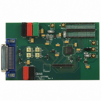
Manufacturer Part Number
EVAL-AD5379EBZ
Description
BOARD EVALUATION FOR AD5379
Manufacturer
Analog Devices Inc
Datasheet
1.AD5379ABCZ.pdf
(28 pages)
Specifications of EVAL-AD5379EBZ
Number Of Dac's
40
Number Of Bits
14
Outputs And Type
40, Single Ended
Sampling Rate (per Second)
50k
Data Interface
Serial, Parallel
Settling Time
20µs
Dac Type
Voltage
Voltage Supply Source
Analog and Digital, Dual ±
Operating Temperature
-40°C ~ 85°C
Utilized Ic / Part
AD5379
Lead Free Status / RoHS Status
Lead free / RoHS Compliant


Table 8. Pin Function Descriptions
Pin
V
V
V
AGND(1–4)
DGND(1–4)
V
V
V
VOUT0 to VOUT39
SER/PAR
SYNC
SCLK
DIN
SDO
DCEN
CS
WR
DB13 to DB0
A0 to A7
REG0
CLR
BUSY
LDAC
CC
SS
DD
REF
REF
BIAS
(1–5)
(1–3)
(1–5)
1(+), V
2(+), V
1
1
1
1
1
REF
REF
1(−)
2(−)
Function
Logic Power Supply; 2.7 V to 5.5 V. These pins should be decoupled with 0.1 μF ceramic capacitors and 10 μF
capacitors.
Negative Analog Power Supply; −11.4 V to −16.5 V for Specified Performance. These pins should be decoupled with
0.1 μF ceramic capacitors and 10 μF capacitors.
Positive Analog Power Supply; +11.4 V to +16.5 V for Specified Performance. These pins should be decoupled with
0.1 μF ceramic capacitors and 10 μF capacitors.
Ground for All Analog Circuitry. All AGND pins should be connected to the AGND plane.
Ground for All Digital Circuitry. All DGND pins should be connected to the DGND plane.
Reference Inputs for DACs 0 to 7, 10 to 17, 20 to 27, and 30 to 37. These voltages are referred to AGND.
Reference Inputs for DACs 8, 9, 18, 19, 28, 29, 38, and 39. These reference voltages are referred to AGND.
DAC Bias Voltage Input/Output. This pin provides an access to the on-chip voltage generator voltage and is provided
for bypassing and overdriving purposes only. If V
higher potential (for example, 5 V). If V
should be decoupled with a 10 nF capacitor to AGND.
DAC Outputs. Buffered analog outputs for each of the 40 DAC channels. Each analog output is capable of driving an
output load of 5 kΩ to ground. Typical output impedance of these amplifiers is 1 Ω.
Interface Select Input. This pin allows the user to select whether the serial or parallel interface is used. This pin has an
internal 1 MΩ pull-down resistor, meaning that the default state at power-on is parallel mode. If this pin is tied high,
the serial interface is used.
Active Low Input. This is the frame synchronization signal for the serial interface.
Serial Clock Input. Data is clocked into the shift register on the falling edge of SCLK. This pin operates at clock speeds
up to 50 MHz.
Serial Data Input. Data must be valid on the falling edge of SCLK.
Serial Data Output. CMOS output. SDO can be used for daisy-chaining a number of devices together. Data is clocked
out on SDO on the rising edge of SCLK and is valid on the falling edge of SCLK.
Daisy-Chain Select Input (Level Sensitive, Active High). When high, this signal is used in conjunction with SER/PAR
high to enable serial interface daisy-chain mode.
Parallel Interface Chip Select Input (Level Sensitive, Active Low). If this pin is low, the device is selected.
Parallel Interface Write Input (Edge Sensitive). The rising edge of WR is used in conjunction with CS low and the
address bus inputs to write to the selected AD5379 registers.
Parallel Data Inputs. The AD5379 can accept a straight 14-bit parallel word on DB0 to DB13, where DB13 is the MSB
and DB0 is the LSB.
Parallel Address Inputs. A7 to A4 are decoded to select one group or multiple groups of registers (input registers, gain
registers (m) or offset registers (c)) for a data transfer. This pin is used in conjunction with the REG1 and REG0 pins to
determine the destination register for the input data. See the Parallel Interface section for details of the address
decoding.
Parallel Interface Register Select Input. This pin is used together with REG1 to select data registers, gain registers,
offset registers, increment/decrement mode, or the soft reset function. See Table 11.
Asynchronous Clear Input (Level Sensitive, Active Low). When CLR is low, the input to each of the DAC output buffer
stages, VOUT0 to VOUT39, is switched to the externally set potential on the relevant REFGND pin. While CLR is low, all
LDAC pulses are ignored. When CLR is taken high again, the DAC outputs remain cleared until LDAC is taken low. The
contents of input registers and DAC registers 0 to 39 are not affected by taking CLR low.
Digital Input/Open-Drain Output. This pin must be pulled high with a pull-up resistor for correct operation. BUSY goes
low during internal calculations of x2. During this time, the user can continue writing new data to additional ×1, c,
and m registers (these are stored in a FIFO), but no further updates to the DAC registers and DAC outputs can take
place. If LDAC is taken low while BUSY is low, this event is stored. Because BUSY is bidirectional, it can be pulled low
externally to delay LDAC action. BUSY also goes low during power-on reset or when the RESET pin is low. During a
RESET operation, the parallel interface is disabled and any events on LDAC are ignored.
Load DAC Logic Input (Active Low). If LDAC is taken low while BUSY is inactive (high), the contents of the input
registers are transferred to the DAC registers and the DAC outputs are updated. If LDAC is taken low while BUSY is
active and internal calculations are taking place, the LDAC event is stored and the DAC registers are updated when
BUSY goes inactive. However, any events on LDAC during power-on reset or RESET are ignored.
REF
Rev. B | Page 13 of 28
(+) < 4.25 V, the on-chip bias generator can be used. In this case, the V
REF
(+) > 4.25 V, V
BIAS
must be pulled high externally to an equal or
AD5379
BIAS
pin
Related parts for EVAL-AD5379EBZ
Image
Part Number
Description
Manufacturer
Datasheet
Request
R


Part Number:
Description:
BOARD EVAL FOR SI270X-A
Manufacturer:
Silicon Laboratories Inc
Datasheet:

Part Number:
Description:
BUCK CONV REF DESIGN KIT IP1201
Manufacturer:
International Rectifier
Datasheet:
Part Number:
Description:
BOARD DEMO SYNC DUAL BUCK CNVTER
Manufacturer:
International Rectifier
Datasheet:
Part Number:
Description:
BOARD DEMO SYNC BUCK CONVETER
Manufacturer:
International Rectifier
Datasheet:

Part Number:
Description:
EVALBOARD/EB Omnidirectional microphone - Analog
Manufacturer:
Analog Devices
Datasheet:
Part Number:
Description:
EVALBOARD/EB Omnidirectional microphone - Analog
Manufacturer:
Analog Devices
Datasheet:


Part Number:
Description:
BOARD EVAL LED DRIVER LT3756
Manufacturer:
Linear Technology
Datasheet:

Part Number:
Description:
BOARD EVAL FOR AD7741/7742
Manufacturer:
Analog Devices Inc
Datasheet:

Part Number:
Description:
±1.7g Dual-Axis IMEMS Accelerometer Evaluation Board
Manufacturer:
Analog Devices Inc
Datasheet:

Part Number:
Description:
IC MULTIPLIER ANALOG 8-SOIC T/R
Manufacturer:
Analog Devices Inc
Datasheet:

Part Number:
Description:
IC ANALOG MULTIPLIER 8-DIP
Manufacturer:
Analog Devices Inc
Datasheet:
Part Number:
Description:
IC ANALOG MULTIPLIER 8-SOIC
Manufacturer:
Analog Devices Inc
Datasheet:
Part Number:
Description:
IC ANALOG MULTIPLIER 8-DIP
Manufacturer:
Analog Devices Inc
Datasheet: