551600003-001A National Semiconductor, 551600003-001A Datasheet - Page 15
551600003-001A
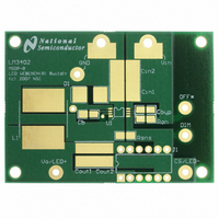
Manufacturer Part Number
551600003-001A
Description
BOARD WEBENCH MSOP LM3402
Manufacturer
National Semiconductor
Series
WEBENCH® Buildit Boardr
Datasheet
1.LM3402MMNOPB.pdf
(28 pages)
Specifications of 551600003-001A
Utilized Ic / Part
LM3402
Lead Free Status / RoHS Status
Lead free / RoHS Compliant
Features
-
Voltage - Output
-
Voltage - Input
-
Current - Output / Channel
-
Outputs And Type
-


INPUT CAPACITORS
Input capacitors at the VIN pin of the LM3402/02HV are se-
lected using requirements for minimum capacitance and rms
ripple current. The input capacitors supply pulses of current
approximately equal to I
are charged up by the input voltage while the power MOSFET
is off. Switching converters such as the LM3402/02HV have
a negative input impedance due to the decrease in input cur-
rent as input voltage increases. This inverse proportionality of
input current to input voltage can cause oscillations (some-
times called ‘power supply interaction’) if the magnitude of the
negative input impedance is greater the the input filter
impedance. Minimum capacitance can be selected by com-
paring the input impedance to the converter’s negative resis-
tance; however this requires accurate calculation of the input
voltage source inductance and resistance, quantities which
can be difficult to determine. An alternative method to select
the minimum input capacitance, C
imum voltage ripple which can be tolerated. This value,Δv
(MAX)
converter on-time, when C
(MIN)
A good starting point for selection of C
voltage ripple of 5% to 10% of V
tance of 2x the C
LM3402/02HV circuits. To determine the rms current rating,
the following formula can be used:
Ceramic capacitors are the best choice for the input to the
LM3402/02HV due to their high ripple current rating, low ESR,
low cost, and small size compared to other types. When se-
lecting a ceramic capacitor, special attention must be paid to
the operating conditions of the application. Ceramic capaci-
tors can lose one-half or more of their capacitance at their
rated DC voltage bias and also lose capacitance with ex-
tremes in temperature. A DC voltage rating equal to twice the
expected maximum input voltage is recommended. In addi-
tion, the minimum quality dielectric which is suitable for
switching power supply inputs is X5R, while X7R or better is
preferred.
RECIRCULATING DIODE
The LM3402/02HV is a non-synchronous buck regulator that
requires a recirculating diode D1 (see the Typical Application
circuit) to carrying the inductor current during the MOSFET
off-time. The most efficient choice for D1 is a Schottky diode
due to low forward drop and near-zero reverse recovery time.
D1 must be rated to handle the maximum input voltage plus
any switching node ringing when the MOSFET is on. In prac-
tice all switching converters have some ringing at the switch-
ing node due to the diode parasitic capacitance and the lead
inductance. D1 must also be rated to handle the average cur-
rent, I
This calculation should be done at the maximum expected
input voltage. The overall converter efficiency becomes more
, is equal to the change in voltage across C
can be selected with the following:
D
, calculated as:
IN(MIN)
I
D
F
= (1 – D) x I
while the power MOSFET is on, and
IN
value is recommended for all
supplies the load current. C
IN
IN(MIN)
. A minimum input capaci-
F
, is to select the max-
IN
is to use an input
IN
during the
IN
IN
15
dependent on the selection of D1 at low duty cycles, where
the recirculating diode carries the load current for an increas-
ing percentage of the time. This power dissipation can be
calculated by checking the typical diode forward voltage, V
from the I-V curve on the product datasheet and then multi-
plying it by I
junction-to-ambient thermal resistance, θ
used to estimate the operating die temperature of the Schot-
tky. Multiplying the power dissipation (P
gives the temperature rise. The diode case size can then be
selected to maintain the Schottky diode temperature below
the operational maximum.
LED CURRENT DURING DIM MODE
The LM3402 contains high speed MOSFET gate drive cir-
cuitry that switches the main internal power MOSFET be-
tween “on” and “off” states. This circuitry uses current derived
from the VCC regulator to charge the MOSFET during turn-
on, then dumps current from the MOSFET gate to the source
(the SW pin) during turn-off. As shown in the block diagram,
the MOSFET drive circuitry contains a gate drive under-volt-
age lockout (UVLO) circuit that ensures the MOSFET remains
off when there is inadequate VCC voltage for proper operation
of the driver. This watchdog circuitry is always running in-
cluding during DIM and shutdown modes, and supplies a
small amount of current from VCC to SW. Because the SW
pin is connected directly to the LEDs through the buck induc-
tor, this current returns to ground through the LEDs. The
amount of current sourced is a function of the SW voltage, as
shown in
Though most power LEDs are designed to run at several
hundred milliamps, some can be seen to glow with a faint light
at extremely low current levels, as low as a couple microamps
in some instances. In lab testing, the forward voltage was
found to be approximately 2V for LEDs that exhibited visible
light at these low current levels. For LEDs that did not show
light emission at very low current levels, the forward voltage
was found to be around 900mV. It is important to remember
that the forward voltage is also temperature dependent, de-
creasing at higher temperatures. Consequently, with a maxi-
mum Vcc voltage of 7.4V, current will be observed in the LEDs
if the total stack voltage is less than about 6V at a forward
current of several microamps. No current is observed if the
stack voltage is above 6V, as shown in
Figure
FIGURE 5. LED Current From SW Pin
D
. Diode datasheets will also provide a typical
5.
Figure
D
JA
= I
, which can be
5. The need for
D
x V
20192157
www.national.com
D
) by θ
D
JA
,
Related parts for 551600003-001A
Image
Part Number
Description
Manufacturer
Datasheet
Request
R

Part Number:
Description:
National Semiconductor [8-Bit D/A Converter]
Manufacturer:
National Semiconductor
Datasheet:
Part Number:
Description:
National Semiconductor [Media Coprocessor]
Manufacturer:
National Semiconductor
Datasheet:
Part Number:
Description:
Digitally Controlled Tone and Volume Circuit with Stereo Audio Power Amplifier, Microphone Preamp Stage and National 3D Sound
Manufacturer:
National Semiconductor
Datasheet:
Part Number:
Description:
Digitally Controlled Tone and Volume Circuit with Stereo Audio Power Amplifier, Microphone Preamp Stage and National 3D Sound
Manufacturer:
National Semiconductor
Datasheet:
Part Number:
Description:
AC97 Rev 2 Codec with Sample Rate Conversion and National 3D Sound
Manufacturer:
National Semiconductor
Part Number:
Description:
Manufacturer:
National Semiconductor
Datasheet:
Part Number:
Description:
Manufacturer:
National Semiconductor
Datasheet:
Part Number:
Description:
General Purpose, Low Voltage, Low Power, Rail-to-Rail Output Operational Amplifiers
Manufacturer:
National Semiconductor
Datasheet:
Part Number:
Description:
8-bit 20 MSPS flash A/D converter.
Manufacturer:
National Semiconductor
Datasheet:
Part Number:
Description:
Low Noise Quad Operational Amplifier
Manufacturer:
National Semiconductor
Datasheet:
Part Number:
Description:
Quad Differential Line Receivers
Manufacturer:
National Semiconductor
Datasheet:
Part Number:
Description:
Quad High Speed Trapezoidal? Bus Transceiver
Manufacturer:
National Semiconductor
Datasheet:
Part Number:
Description:
Dual Line Receiver
Manufacturer:
National Semiconductor
Datasheet:
Part Number:
Description:
TTL to 10k ECL Level Translator with Latch
Manufacturer:
National Semiconductor
Datasheet: