NCP3065SOBCKGEVB ON Semiconductor, NCP3065SOBCKGEVB Datasheet - Page 13
NCP3065SOBCKGEVB
Manufacturer Part Number
NCP3065SOBCKGEVB
Description
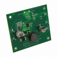
EVAL BOARD FOR NCP3065SOBCKG
Manufacturer
ON Semiconductor
Datasheets
1.NCP3065DR2G.pdf
(18 pages)
2.NCP30653ABCKGEVB.pdf
(18 pages)
3.NCP3065SOBCKGEVB.pdf
(1 pages)
Specifications of NCP3065SOBCKGEVB
Design Resources
NCP3065 Buck Eval Board BOM NCP3065SOBCKGEVB Gerber Files NCP3065 Buck Eval Board Schematic
Current - Output / Channel
350mA
Outputs And Type
1, Non-Isolated
Voltage - Output
3.6V
Voltage - Input
12V
Utilized Ic / Part
NCP3065
Core Chip
NCP3065
Topology
Buck-Boost
Development Tool Type
Hardware - Eval/Demo Board
Leaded Process Compatible
Yes
Mcu Supported Families
NCP3065
Peak Reflow Compatible (260 C)
Yes
Rohs Compliant
Yes
Lead Free Status / RoHS Status
Lead free / RoHS Compliant
Features
-
Lead Free Status / Rohs Status
Lead free / RoHS Compliant
For Use With/related Products
NCP3065SOBCKG
Other names
NCP3065SOBCKGEVBOS


Pulse feedback design
is similar but not exactly the same as a hysteretic
architecture. The output switching frequency is dependent
on the input and output conditions. The NCP3065 oscillator
generates a constant frequency that is set by an external
capacitor. This output signal is then gated by the peak
current comparator and the oscillator. When the output
current is above the threshold voltage the switch turns off.
When the output current is below the threshold voltage the
switch is turned on and gated with the oscillator. A
simplified schematic is shown in Figure 18. This may cause
possible overshoots on the output. Using the pulse feedback
The NCP3065 is a burst−mode architecture product which
Figure 15. NCP3065 Behavior with Dimming,
Frequency is 200 Hz, Duty Cycle 50%
Figure 17. Output Current Dependency on the Dimming Duty Cycle
800
700
600
500
400
300
200
100
0
0
10
20
30
http://onsemi.com
40
DUTY CYCLE (%)
50
13
circuit will reduce this overshoot. This will result in a
stabilized switching frequency and reduce the overshoot and
output ripple. The pulse feedback circuit is implemented by
adding an external resistor R8 between the CT pin and
inductor input as shown in the buck schematic Figure 8.
conditions and switching frequency. The typical range is 3k
to 200k. Table 1 contains a list of typical applications and the
recommended value for the pulse feedback resistor. Using
an adjustable resistor in place of R8 when evaluating an
application will allow the designer to optimize the value and
make a final selection.
V
12 V
F
60
The resistor value is dependent on the input/output
3.6 V
IN
V
24 V
70
,
F
Figure 16. NCP3065 Dimming Behavior,
3.6 V
IN
Frequency 1 kHz, Duty Cycle 50%
V
,
24 V
80
F
7.2 V
IN
90
,
100
Related parts for NCP3065SOBCKGEVB
Image
Part Number
Description
Manufacturer
Datasheet
Request
R

Part Number:
Description:
Up to 1.5 A Constant Current Switching Regulator for LEDs
Manufacturer:
ON Semiconductor
Datasheet:

Part Number:
Description:
EVAL BOARD FOR NCP3065SOBSTG
Manufacturer:
ON Semiconductor
Datasheet:

Part Number:
Description:
EVAL BOARD FOR NCP30653ABCKG
Manufacturer:
ON Semiconductor
Datasheet:
Part Number:
Description:
ON Semiconductor [VOLTAGE REGULATOR]
Manufacturer:
ON Semiconductor
Datasheet:
Part Number:
Description:
357-036-542-201 CARDEDGE 36POS DL .156 BLK LOPRO
Manufacturer:
ON Semiconductor
Datasheet:
Part Number:
Description:
357-036-542-201 CARDEDGE 36POS DL .156 BLK LOPRO
Manufacturer:
ON Semiconductor
Datasheet:
Part Number:
Description:
357-036-542-201 CARDEDGE 36POS DL .156 BLK LOPRO
Manufacturer:
ON Semiconductor
Datasheet:
Part Number:
Description:
357-036-542-201 CARDEDGE 36POS DL .156 BLK LOPRO
Manufacturer:
ON Semiconductor
Datasheet:
Part Number:
Description:
357-036-542-201 CARDEDGE 36POS DL .156 BLK LOPRO
Manufacturer:
ON Semiconductor
Datasheet:
Part Number:
Description:
357-036-542-201 CARDEDGE 36POS DL .156 BLK LOPRO
Manufacturer:
ON Semiconductor
Datasheet:
Part Number:
Description:
357-036-542-201 CARDEDGE 36POS DL .156 BLK LOPRO
Manufacturer:
ON Semiconductor
Datasheet:
Part Number:
Description:
357-036-542-201 CARDEDGE 36POS DL .156 BLK LOPRO
Manufacturer:
ON Semiconductor
Datasheet:
Part Number:
Description:
357-036-542-201 CARDEDGE 36POS DL .156 BLK LOPRO
Manufacturer:
ON Semiconductor
Datasheet:
Part Number:
Description:
357-036-542-201 CARDEDGE 36POS DL .156 BLK LOPRO
Manufacturer:
ON Semiconductor
Datasheet: