LX1991-03EVAL Microsemi Analog Mixed Signal Group, LX1991-03EVAL Datasheet - Page 4
LX1991-03EVAL
Manufacturer Part Number
LX1991-03EVAL
Description
BOARD EVAL LED DRIVER 6 CHANNEL
Manufacturer
Microsemi Analog Mixed Signal Group
Specifications of LX1991-03EVAL
Current - Output / Channel
30mA
Outputs And Type
6, Non-Isolated
Voltage - Output
40V
Features
Dimmable
Voltage - Input
4.5 ~ 5.5V
Utilized Ic / Part
LX1991
Lead Free Status / RoHS Status
Lead free / RoHS Compliant


LX1991 E
logic can be applied to this point to disable the
device. This external signal must be able to
drive the 10K pull-up resistor low (less than
0.8V).The PWM_IN header input allows an
external PWM signal to control the output
current by duty cycle dimming. This is
accomplished
DIG_DIM input with a logic signal.
practical limit to this switching frequency is
about 100Khz, at frequencies greater than this
internal delays will add errors to the expected
output duty cycle. The evaluation board comes
with a 470pF CSLOPE capacitor. This value
can be increased to vary the rise and fall times
of the output current waveform. For greater
detail see the LX1991 datasheet.
Test Points SINK1 to SINK6 allow you to
monitor the voltage drop across these pins to
ground. This voltage will change to maintain the
Copyright © 2002
Rev. 1.0 1/8/03
Jumper
PWM_IN
EXT_EN
RTN/GND
EXT VDD
An external voltage signal or open collector
PWM_IN
EXT_EN
VLOAD
SINK1
SINK2
SINK3
SINK4
SINK5
SINK6
Point
Test
Jumper to PULLUP connects PWM_IN through a 10K pull-up resistor to EXT VDD, Jumper
to RTN connects PWM_IN to Ground. Open allows hookup to external PWM source.
Jumper to RTN disables the LX1991 by pulling down on the 10K pull-up resistor ; EXT_EN
open enable the LX1991 through the 10K pull-up to EXT VDD
VALUATION
VLOAD Input, power supply to LED’s (3 to 40V)
Common Ground Reference
VDD Input to LX1991 (4.5 to 5.5V)
ENABLE input can be connected to external enable signal; high or floating is on, low is
off (LX1991 pin 16)
SINK1 (LX1991 pin 3)
SINK2 (LX1991 pin 4)
SINK3 (LX1991 pin 6)
SINK4 (LX1991 pin 7)
SINK5 (LX1991 pin 8)
SINK6 (LX1991 pin 10)
PWM Input can be connected to external pulse generator for duty cycle dimming
(LX1991 pin 1)
by
switching
B
11861 Western Avenue, Garden Grove, CA. 92841, 714-898-8121, Fax: 714-893-2570
OARD
the
Table 3 – Test Point Descriptions
Table 2 – Jumper Explanation
device’s
The
Integrated Products
Microsemi
Description
Function
correct forward voltage across the LED’s for the
programmed sink current. It can range from as
low as 400mV to 40V when the outputs are off
depending on the VLOAD supply voltage.
The various jumper positions are summarized in
table 2 and test points in table 3. The factory
installed active and passive components list can
be found in table 4. Following the two tables
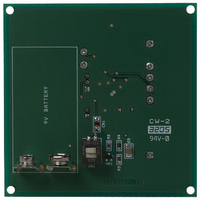
you will find the PCB silkscreen figure 1 and the
circuit schematic in figure 2. All necessary PCB
traces and components are on the topside of the
board.
silkscreen on the bottom side that when
populated is used for a special version of the
evaluation board that is used internally by
Microsemi
purposes.
However there are PCB traces and
for
training
and
U
demonstration
SER
G
UIDE
Page 4
Related parts for LX1991-03EVAL
Image
Part Number
Description
Manufacturer
Datasheet
Request
R

Part Number:
Description:
KIT EVALUATION FOR LED DRIVER
Manufacturer:
Microsemi Analog Mixed Signal Group
Datasheet:

Part Number:
Description:
BOARD EVAL LED DRIVER 6CHANNEL
Manufacturer:
Microsemi Analog Mixed Signal Group
Datasheet:

Part Number:
Description:
IC USB LINE TERM EMI/ESD SC70-6
Manufacturer:
Microsemi Analog Mixed Signal Group
Datasheet:
Part Number:
Description:
IC USB LINE TERM EMI/ESD SC70-6
Manufacturer:
Microsemi Analog Mixed Signal Group
Datasheet:

Part Number:
Description:
IC TERM SCSI 9LINE MODE 24TSSOP
Manufacturer:
Microsemi Analog Mixed Signal Group
Datasheet:

Part Number:
Description:
IC TERM SCSI 9LINE MODE 28TSSOP
Manufacturer:
Microsemi Analog Mixed Signal Group
Datasheet:

Part Number:
Description:
IC TERM SCSI 9LINE LVD 24TSSOP
Manufacturer:
Microsemi Analog Mixed Signal Group
Datasheet:
Part Number:
Description:
IC TERM SCSI 9LINE MODE 36QSOP
Manufacturer:
Microsemi Analog Mixed Signal Group
Datasheet:

Part Number:
Description:
IC USB LINE TERM EMI/ESD SOT23-6
Manufacturer:
Microsemi Analog Mixed Signal Group
Datasheet:

Part Number:
Description:
IC USB LINE TERM EMI/ESD SOT23-6
Manufacturer:
Microsemi Analog Mixed Signal Group
Datasheet:

Part Number:
Description:
IC USB EMI FLTR ESD PROT SOT23-6
Manufacturer:
Microsemi Analog Mixed Signal Group
Part Number:
Description:
IC USB LINE TERM EMI/ESD SOT23-6
Manufacturer:
Microsemi Analog Mixed Signal Group
Datasheet:
Part Number:
Description:
IC AMP AUDIO PWR 10W STER 44SSOP
Manufacturer:
Microsemi Analog Mixed Signal Group
Datasheet:

Part Number:
Description:
IC CHARGER BATT USB LI-ION 20MLP
Manufacturer:
Microsemi Analog Mixed Signal Group
Datasheet:

Part Number:
Description:
IC LED DRIVER LINEAR 6-MLP
Manufacturer:
Microsemi Analog Mixed Signal Group
Datasheet: