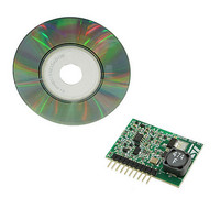
EVL6562A-LED STMicroelectronics, EVL6562A-LED Datasheet

EVL6562A-LED
Specifications of EVL6562A-LED
Available stocks
Related parts for EVL6562A-LED
EVL6562A-LED Summary of contents
Page 1
Features REALISED IN BCD TECHNOLOGY ■ TRANSITION-MODE CONTROL OF PFC PRE- ■ REGULATORS PROPRIETARY MULTIPLIER DESIGN FOR ■ MINIMUM THD OF AC INPUT CURRENT VERY PRECISE ADJUSTABLE OUTPUT ■ OVERVOLTAGE PROTECTION ULTRA-LOW (≤70µA) START-UP CURRENT ■ LOW (≤4 mA) ...
Page 2
L6562 2 Description (continued) The highly linear multiplier includes a special circuit, able to reduce AC input current distortion, that allows wide-range-mains operation with an extremely low THD, even over a large load range. The output voltage is controlled by ...
Page 3
Table 4. Pin Description N° Pin 1 INV Inverting input of the error amplifier. The information on the output voltage of the PFC pre- regulator is fed into the pin through a resistor divider. 2 COMP Output of the error ...
Page 4
L6562 Table 5. Electrical Characteristics (continued -25 to 125° 12 Symbol Parameter G Voltage Gain v GB Gain-Bandwidth Product I Source Current COMP Sink Current V Upper Clamp Voltage COMP Lower Clamp Voltage ...
Page 5
Typical Electrical Characteristics Figure 4. Supply current vs. Supply voltage I CC (mA 0.5 0.1 0.05 0.01 0.005 cc(V) Figure 5. Start-up & UVLO vs. T 12.5 V CC-ON (V) 12 ...
Page 6
L6562 Figure 8. Feedback reference vs REF 2.6 (V) 2.55 2.5 2.45 2.4 - (°C) Figure 9. OVP current vs OVP 41 (µA) 40.5 40 39 (°C) ...
Page 7
Figure 14. Vcs clamp vs CSx 2 (V) 1.8 1.6 1.4 Vcc = Upper clamp COMP 1 (°C) Figure 15. Start-up timer vs. T Tstart 150 (µs) Vcc ...
Page 8
L6562 Figure 20. Gate-drive clamp vs. T Vpin7 clamp (°C) 4 Application Information 4.1 Overvoltage protection Under steady-state conditions, the voltage control loop keeps the output voltage Vo of ...
Page 9
When the load of a PFC pre-regulator is very low, the output voltage tends to stay steadily above the nom- inal value, which cannot be handled by the Dynamic OVP. If this occurs, however, the error amplifier out- put will ...
Page 10
L6562 the output of the multiplier in the proximity of the line voltage zero-crossings. This offset is reduced as the instantaneous line voltage increases, so that it becomes negligible as the line voltage moves toward the top of the sinusoid. ...
Page 11
Figure 25. EVAL6562-80W: PCB and component layout (Top view, real size 108 mm) Table 6. EVAL6562N: Evaluation results at full load Vin (V ) Pin ( 86.4 110 84.6 135 83.8 175 83.2 220 ...
Page 12
L6562 Table 8. EVAL6562N: No-load measurements Vin (V ) Pin ( 110 135 (*) 175 (*) 220 (*) 265 (*) Vcc = 12V supplied externally Figure 26. Line filter (not tested for EMI compliance) used for EVAL6562N evaluation ...
Page 13
Package Information In order to meet environmental requirements, ST offers these devices in ECOPACK packages have a Lead-free second level interconnect. The category of second Level Interconnect is marked on the package and on the inner box label, in ...
Page 14
L6562 Figure 28. SO-8 Mechanical Data & Package Dimensions mm DIM. MIN. TYP. A 1.35 A1 0.10 A2 1.10 B 0.33 C 0.19 (1) 4. 3.80 e 1.27 H 5.80 h 0.25 L 0.40 k 0˚ (min.), 8˚ ...
Page 15
Revision History Table 9. Revision History Date Revision January 2004 June 2004 May 2005 November 2005 5 First Issue 6 Modified the Style-look in compliance with the “Corporate Technical Publications Design Guide”. Changed input of the power amplifier connected ...
Page 16
... No license is granted by implication or otherwise under any patent or patent rights of STMicroelectronics. Specifications mentioned in this publication are subject to change without notice. This publication supersedes and replaces all information previously supplied. STMicroelectronics products are not authorized for use as critical components in life support devices or systems without express written approval of STMicroelectronics ...


