LM27965SQEV National Semiconductor, LM27965SQEV Datasheet - Page 11
LM27965SQEV
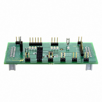
Manufacturer Part Number
LM27965SQEV
Description
BOARD EVALUATION LM27965SQ
Manufacturer
National Semiconductor
Series
PowerWise®r
Datasheet
1.LM27965SQ-MXNOPB.pdf
(14 pages)
Specifications of LM27965SQEV
Current - Output / Channel
20mA
Outputs And Type
9, Non-Isolated
Voltage - Output
4 V
Features
Charge Pump
Voltage - Input
2.7 ~ 5.5V
Utilized Ic / Part
LM27965
Lead Free Status / RoHS Status
Not applicable / Not applicable


The statement above is a simple example of the LED drive
capabilities of the LM27965. The statement contains the key
application parameters that are required to validate an LED-
drive design using the LM27965: LED current (I
of active LEDs (N
mum input voltage (V
The equation below can be used to estimate the maximum
output current capability of the LM27965:
I
the other LED banks.
R
losses of the charge pump that result in voltage droop at the
pump output P
is proportional to the total output current of the charge pump,
the loss parameter is modeled as a resistance. The output
resistance of the LM27965 is typically 2.75Ω (V
= 25°C). In equation form:
k
mum voltage required to be present across the current sinks
for them to regulate properly. This minimum voltage is pro-
portional to the programmed LED current, so the constant has
units of mV/mA. The typical k
In equation form:
The "I
R
ing for I
minimum input voltage and LED forward voltage. Output cur-
rent capability can be increased by raising the minimum input
voltage of the application, or by selecting an LED with a lower
forward voltage. Excessive power dissipation may also limit
output current capability of an application.
Total Output Current Capability
The maximum output current that can be drawn from the
LM27965 is 180mA. Each driver bank has a maximum allotted
current per Dxx sink that must not be exceeded.
The 180mA load can be distributed in many different config-
urations. Special care must be taken when running the
LM27965 at the maximum output current to ensure proper
functionality.
PARALLEL CONNECTED AND UNUSED OUTPUTS
Outputs D1A-5A or D1B-D3B may be connected together to
drive one or two LEDs at higher currents. In such a configu-
ration, all five parallel current sinks (BankA) of equal value
can drive a single LED. The LED current programmed for
BankA should be chosen so that the current through each of
the outputs is programmed to 20% of the total desired LED
ADDITIONAL
HR
OUT
OUT
V
I
LED_MAX
I
POUT
– Headroom constant. This parameter models the mini-
LED_MAX
– Output resistance. This parameter models the internal
equation (eq. 2) with the k
LED-MAX
DRIVER TYPE
LEDx
= (1.5 × V
(V
is the additional current that could be delivered to
Typical Headroom Constant Values
. Maximum LED current is highly dependent on
POUT
= [(1.5 x V
DxA
DxB
DxC
" equation (eq. 1) is obtained from combining the
= [(1.5 x V
OUT
[(N
– V
. Since the magnitude of the voltage droop
x
), LED forward voltage (V
IN
x
[(N
LEDx
) – [(N
x R
IN-MIN
k
k
IN
x
HRA
HRB
IN
x 2.75Ω) + k
OUT
) > k
) - V
) - V
).
(eq. 2)
A
= 8mV/mA
= 8mV/mA
) + k
× I
LED
HRx
LED
HR
LEDA
HRx
MAXIMUM Dxx CURRENT
of the LM27965 is 8mV/mA.
HRx
- (I
× I
- (I
equation (eq. 3) and solv-
LEDx
] (eq. 1)
ADDITIONAL
+ N
ADDITIONAL
30mA per DxA Pin
30mA per DxB Pin
30mA per DxB Pin
HRx
B
]
× I
LEDB
(eq. 3)
LED
× 2.75Ω)] /
× R
LEDx
IN
), and mini-
) × R
= 3.6V, T
OUT
), number
)] /
OUT
]
A
11
current. For example, if 60mA is the desired drive current for
a single LED, R
through each of the current sink inputs is 12mA.
Connecting the outputs in parallel does not affect internal op-
eration of the LM27965 and has no impact on the Electrical
Characteristics and limits previously presented. The available
diode output current, maximum diode voltage, and all other
specifications provided in the Electrical Characteristics table
apply to this parallel output configuration, just as they do to
the standard 5-LED application circuit.
Both BankA and BankB utilize LED forward voltage sensing
circuitry on each Dxx pin to optimize the charge-pump gain
for maximum efficiency. Due to the nature of the sensing cir-
cuitry, it is not recommended to leave any of the DxA (D1A-
D4A) or DxB (D1B-D2B) pins open if either diode bank is
going to be used during normal operation. Leaving DxA and/
or DxB pins unconnected will force the charge-pump into 3/2×
mode over the entire V
that could have been achieved by switching to 1× mode at
higher input voltages.
If D5A is not used, it is recommended that the driver pin be
grounded and the general purpose register bit EN5A be set
to 0 to ensure proper gain transitions.
The D3B driver can be completely turned on or off on the fly
using the general purpose register. The diode monitoring cir-
cuity is enabled and disabled with the driver. If D3B is not
used, it is recommended that the driver pin be grounded and
the general purpose register bit EN3B be set to 0 to ensure
proper gain transitions.
Care must be taken when selecting the proper R
The current on any Dxx pin must not exceed the maximum
current rating for any given current sink pin.
POWER EFFICIENCY
Efficiency of LED drivers is commonly taken to be the ratio of
power consumed by the LEDs (P
the input of the part (P
input current is equal to the charge pump gain times the output
current (total LED current). The efficiency of the LM27965 can
be predicted as follows:
The LED voltage is the main contributor to the charge-pump
gain selection process. Use of low forward-voltage LEDs
(3.0V- to 3.5V) will allow the LM27965 to stay in the gain of
1× for a higher percentage of the lithium-ion battery voltage
range when compared to the use of higher forward voltage
LEDs (3.5V to 4.0V). See the LED Forward Voltage Monitor-
ing section of this datasheet for a more detailed description
of the gain selection and transition process.
For an advanced analysis, it is recommended that power con-
sumed by the circuit (V
rather than power efficiency.
POWER DISSIPATION
The power dissipation (P
can be approximated with the equations below. P
power generated by the 3/2× - 1× charge pump, P
power consumed by the LEDs, T
and θ
LLP-24 package. V
JA
is the junction-to-ambient thermal resistance for the
(V
P
P
LEDB
LEDTOTAL
IN
SET
= V
× N
E = (P
should be selected such that the current
IN
IN
B
IN
× (GAIN × I
is the input voltage to the LM27965,
IN
IN
P
= (V
× I
). With a 3/2× - 1× charge pump, the
IN
DISS
range negating any efficiency gain
x I
LEDTOTAL
LEDB
= V
LEDA
IN
) and junction temperature (T
) for a given load be evaluated
IN
) + (V
A
× N
× I
is the ambient temperature,
LED
LEDTOTAL
÷ P
IN
A
LEDC
) to the power drawn at
× I
IN
)
LEDA
× I
+ I
LEDC
) +
Q
)
)
www.national.com
SET
LED
IN
value.
is the
is the
J
)
Related parts for LM27965SQEV
Image
Part Number
Description
Manufacturer
Datasheet
Request
R

Part Number:
Description:
Accurate, 120 C-150 C Factory Preset Thermostat Lm27 Form
Manufacturer:
National Semiconductor Corporation
Datasheet:

Part Number:
Description:
Factory Preset Thermostat
Manufacturer:
National Semiconductor
Datasheet:
Part Number:
Description:
National Semiconductor [8-Bit D/A Converter]
Manufacturer:
National Semiconductor
Datasheet:
Part Number:
Description:
National Semiconductor [Media Coprocessor]
Manufacturer:
National Semiconductor
Datasheet:
Part Number:
Description:
Digitally Controlled Tone and Volume Circuit with Stereo Audio Power Amplifier, Microphone Preamp Stage and National 3D Sound
Manufacturer:
National Semiconductor
Datasheet:
Part Number:
Description:
Digitally Controlled Tone and Volume Circuit with Stereo Audio Power Amplifier, Microphone Preamp Stage and National 3D Sound
Manufacturer:
National Semiconductor
Datasheet:
Part Number:
Description:
AC97 Rev 2 Codec with Sample Rate Conversion and National 3D Sound
Manufacturer:
National Semiconductor
Part Number:
Description:
Manufacturer:
National Semiconductor
Datasheet:
Part Number:
Description:
Manufacturer:
National Semiconductor
Datasheet:
Part Number:
Description:
General Purpose, Low Voltage, Low Power, Rail-to-Rail Output Operational Amplifiers
Manufacturer:
National Semiconductor
Datasheet:
Part Number:
Description:
8-bit 20 MSPS flash A/D converter.
Manufacturer:
National Semiconductor
Datasheet:
Part Number:
Description:
Low Noise Quad Operational Amplifier
Manufacturer:
National Semiconductor
Datasheet:
Part Number:
Description:
Quad Differential Line Receivers
Manufacturer:
National Semiconductor
Datasheet:
Part Number:
Description:
Quad High Speed Trapezoidal? Bus Transceiver
Manufacturer:
National Semiconductor
Datasheet: