LP3944ISQEV National Semiconductor, LP3944ISQEV Datasheet - Page 5
LP3944ISQEV
Manufacturer Part Number
LP3944ISQEV
Description
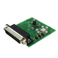
BOARD EVALUATION LP3944ISQ
Manufacturer
National Semiconductor
Series
PowerWise®r
Specifications of LP3944ISQEV
Current - Output / Channel
25mA
Outputs And Type
8, Non-Isolated
Features
Dimmable, I²C Interface
Voltage - Input
2.3 ~ 5.5 V
Utilized Ic / Part
LP3944
Core Chip
LP3944
No. Of Outputs
8
Output Current
25mA
Dimming Control Type
I2C
Kit Contents
Board, User Guide
Development Tool Type
Hardware - Eval/Demo Board
Lead Free Status / RoHS Status
Not applicable / Not applicable
Voltage - Output
-


I
t
t
t
t
t
t
t
2
CLK-LP
CLK-HP
SU
DATA-HOLD
DATA-SU
SU
TRANS
Symbol
Electrical Characteristics
Unless otherwise noted, V
in boldface type apply over the entire junction temperature range for operation, T
Note 1: Absolute Maximum Ratings are limits beyond which damage to the device may occur. Operating Ratings are conditions under which operation of the device
is guaranteed. Operating Ratings do not imply guaranteed performance limits. For guaranteed performance limits and associated test conditions, see the Electrical
Characteristics tables.
Note 2: All voltages are with respect to the potential at the GND pin.
Note 3: The Absolute Maximum power dissipation depends on the ambient temperature and can be calculated using the formula
where T
Absolute Maximum Ratings results from substituting the Absolute Maximum junction temperature, 150˚C, for T
be dissipated safely at ambient temperature below 85˚C. Less power can be dissipated safely at ambient temperatures above 85˚C. The Absolute Maximum power
dissipation can be increased by 27 mW for each degree below 85˚C, and it must be de-rated by 27 mW for each degree above 85˚C. For Operating Ratings
maximum power dissipation, T
Note 4: The human-body model is 100 pF discharged through 1.5 kΩ. The machine model is 0Ω in series with 220 pF.
Note 5: Limits are guaranteed. All electrical characteristics having room-temperature limits are tested during production with T
guaranteed by correlating the electrical characteristics to process and temperature variations and applying statistical process control.
Note 6: Each LED pin should not exceed 25 mA and the package should not exceed a total of 200 mA.
Note 7: Guaranteed by design.
Typical Performance Characteristics
C INTERFACE (SCL AND SDA PINS)
P = (T
J
is the junction temperature, T
J
CLK Low Period
CLK High Period
Set-Up Time Repeated
START Condition
Data Hold Time
Data Set-Up Time
Set-Up Time for STOP
Condition
Maximum Pulse Width of
Spikes that Must Be
Suppressed by the Input
Filter of Both DATA & CLK
Signals
— T
A
)/θ
JA
,
Parameter
(1)
J
= 125˚C and T
DD
= 5.5V. Typical values and limits appearing in normal type apply for T
A
is the ambient temperature, and θ
A
= 85˚C
(Continued)
(Note 7)
(Note 7)
(Note 7)
(Note 7)
(Note 7)
(Note 7)
(Note 7)
(T
Frequency vs. Temp
Conditions
V
A
DD
= −40˚C to +85˚C),
= 2.3V to 3.0V
JA
is the junction-to-ambient thermal resistance. The 1.76W rating appearing under
5
Typical
20085317
50
J
= −40˚C to +125˚C. (Note 5)
J
, 85˚C for T
Min
300
100
1.3
0.6
0.6
0.6
A
, and 37˚C/W for θ
J
J
= 25˚C. All hot and cold limits are
Limit
= 25˚C. Limits appearing
Max
JA
. More power can
www.national.com
Units
µs
µs
µs
ns
ns
µs
ns
Related parts for LP3944ISQEV
Image
Part Number
Description
Manufacturer
Datasheet
Request
R

Part Number:
Description:
National Semiconductor [8-Bit D/A Converter]
Manufacturer:
National Semiconductor
Datasheet:
Part Number:
Description:
National Semiconductor [Media Coprocessor]
Manufacturer:
National Semiconductor
Datasheet:
Part Number:
Description:
Digitally Controlled Tone and Volume Circuit with Stereo Audio Power Amplifier, Microphone Preamp Stage and National 3D Sound
Manufacturer:
National Semiconductor
Datasheet:
Part Number:
Description:
Digitally Controlled Tone and Volume Circuit with Stereo Audio Power Amplifier, Microphone Preamp Stage and National 3D Sound
Manufacturer:
National Semiconductor
Datasheet:
Part Number:
Description:
AC97 Rev 2 Codec with Sample Rate Conversion and National 3D Sound
Manufacturer:
National Semiconductor
Part Number:
Description:
Manufacturer:
National Semiconductor
Datasheet:
Part Number:
Description:
Manufacturer:
National Semiconductor
Datasheet:
Part Number:
Description:
General Purpose, Low Voltage, Low Power, Rail-to-Rail Output Operational Amplifiers
Manufacturer:
National Semiconductor
Datasheet:
Part Number:
Description:
8-bit 20 MSPS flash A/D converter.
Manufacturer:
National Semiconductor
Datasheet:
Part Number:
Description:
Low Noise Quad Operational Amplifier
Manufacturer:
National Semiconductor
Datasheet:
Part Number:
Description:
Quad Differential Line Receivers
Manufacturer:
National Semiconductor
Datasheet:
Part Number:
Description:
Quad High Speed Trapezoidal? Bus Transceiver
Manufacturer:
National Semiconductor
Datasheet:
Part Number:
Description:
Dual Line Receiver
Manufacturer:
National Semiconductor
Datasheet:
Part Number:
Description:
TTL to 10k ECL Level Translator with Latch
Manufacturer:
National Semiconductor
Datasheet: