NCP5050GEVB ON Semiconductor, NCP5050GEVB Datasheet

EVAL BOARD FOR NCP5050G

NCP5050GEVB

Manufacturer Part Number
NCP5050GEVB
Description
EVAL BOARD FOR NCP5050G
Manufacturer
ON Semiconductor
Datasheets

Specifications of NCP5050GEVB

Design Resources
NCP5050 EVB BOM NCP5050 EVB Schematic NCP5050GEVB Gerber Files
Current - Output / Channel
Adjustable
Outputs And Type
1, Non-Isolated
Voltage - Output
Up to 20V
Features
Dimmable
Voltage - Input
2.7 ~ 5.5 V
Utilized Ic / Part
NCP5050
Core Chip
NCP5050
Topology
Boost
No. Of Outputs
1
Dimming Control Type
PWM
Development Tool Type
Hardware - Eval/Demo Board
Leaded Process Compatible
Yes
Mcu Supported Families
NCP5050
Rohs Compliant
Yes
Lead Free Status / RoHS Status
Lead free / RoHS Compliant
For Use With/related Products
NCP5050G
Other names
NCP5050GEVBOS
NCP5050
4.5 W Flash White LED
Boost Driver
converter optimized for constant current applications such as driving
high−powered white LEDs. This device has been designed with
high−efficiency for use in portable applications and is capable of
driving up to 5 high power LEDs in series for camera flash or
flashlight (torch) applications. To support the need of driving the
LEDs in a high current pulse mode for flash as well as a continuous
mode for focus or torch, a control pin and support circuitry is
incorporated which allows the user to program two LED currents. The
both output current are fully configurable via the use of 2 external
resistors and this average current can be reduced by applying a PWM
signal to the CTRL pin up to 50 kHz.
inductors and ceramic capacitors. In addition the compensation is
internal to the device which simplifies the design and reduces the PCB
component count. To protect the device cycle−by−cycle current
limiting and a thermal shutdown circuit have been incorporated as
well as output over−voltage and time out protection. The maximum
peak current level of the power switch is adjustable to allow further
system optimization. The NCP5050 is housed in a low profile space
efficient 3x3 mm thermally enhanced WDFN.
Features
Typical Applications
© Semiconductor Components Industries, LLC, 2010
December, 2010 − Rev. 1
The NCP5050 is a high powered fixed frequency PWM boost
The PWM operates at 1.7 MHz which allows the use of small
High Efficiency Up to 88% for 2 LED (V
White LED Flash (Camera Phone, Digital Still Camera,
Personal Media Player)
Details)
ENABLE
High frequency Dimming PWM Control
Maximum V
1.7 MHz PWM DC/DC Converter
Shut Down Control Facility with True−Cutoff
Open LED (Output Overvoltage) Protection
1.2 s Timer out Function
Soft Start to Limit Inrush Current
Small 3x3x0.8 mm WDFN Package
These are Pb−Free Devices
Portable Flash Lights
Medium Size LCD Backlight (See Application Note AND8294/D for
FLASH/
TORCH
4.7 mF
2.8 k
C1
R1
2.7 to 5.5 V
Figure 1. Typical Application Circuit
out
9
5
3
4
NCP5050
PVIN
PCA
CTRL
HCM
of 20 V
2.0
2.2 mH
L1
R
HCS
R2
SW
VS
FB
R3
R
LCS
10
2
7
10.0
D1
F
= 3.5 V by LED) at 200 mA
D2
D6
L1: TDK VLF5012T−2R2
D1: ON MBR130LSF
C1: 4.7 mF 6.3 V 0603
TDK C1608X5R0J475M
TDK C2012X5R1E105M
C2: 1 mF 25V 0805
C2
1 mF
1
See detailed ordering and shipping information in the package
dimensions section on page 13 of this data sheet.
PGND
CTRL
WDFN10, 3x3
CASE 522AA
PCA
A
L
Y
W
G
(Note: Microdot may be in either location)
CM
ISSUE A
VS
ORDERING INFORMATION
1
2
3
4
5
PIN CONNECTIONS
http://onsemi.com
= Assembly Location
= Wafer Lot
= Year
= Work Week
= Pb−Free Package
(Top View)
Publication Order Number:
MARKING
DIAGRAM
ALYWG
5050
10
9
8
7
6
G
NCP5050/D
SW
PVIN
LCS
FB
HCS

Related parts for NCP5050GEVB

NCP5050GEVB Summary of contents

Page 1

NCP5050 4.5 W Flash White LED Boost Driver The NCP5050 is a high powered fixed frequency PWM boost converter optimized for constant current applications such as driving high−powered white LEDs. This device has been designed with high−efficiency for use in ...

Page 2

Figure 2. Typical Efficiency 2 4.7 mF 0603 6.3 V OSC Thermal 1.7MHz Shut down PCA 5 R1 PWM CONTROLLER 2.8k CTRL 3 Band Gap ...

Page 3

PIN FUNCTION DESCRIPTION Pin Name Pin Type 1 PGND POWER Power Ground: This pin is the power ground and carries the high switching current. A high quality ground must be provided to avoid any noise spikes/uncontrolled operation. Cares must be ...

Page 4

MAXIMUM RATINGS (Note 1) Rating Power Supply Voltage (Note 2) Over Voltage Protection Human Body Model (HBM) ESD Rating (Note 3) HCS and FB Pins Machine Model (MM) ESD Rating (Note 3) HCS and FB Pins Digital Input Voltage Digital ...

Page 5

ELECTRICAL CHARACTERISTICS to 5.5 V (Unless otherwise noted). Typical values are referenced to T Characteristics Operating Power Supply Maximum Inductor Current (Notes 9 and 11) (see Figure 24) Refer Switch Current Limit section @ 25°C Power Switch ON Resistor T ...

Page 6

TYPICAL OPERATING CHARACTERISTICS 1000 800 600 3.3 V 400 in 200 Operating Area (V) out Figure 4. Maximum Output Current Available vs. V ...

Page 7

TYPICAL OPERATING CHARACTERISTICS Channel 1:V OUT DC Measurement, 5 V/Div Channel 2:V OUT AC Measurement, 500 mV/Div Figure 10. Typical V Ripple in OVP OUT Condition, No Load Channel 1:SW Pin DC Measurement, 5 V/Div Channel 4:LED Current DC Measurement, ...

Page 8

TYPICAL OPERATING CHARACTERISTICS 50.0 45.0 40.0 35.0 30.0 25.0 20.0 15.0 10.0 5.0 0 DUTY CYCLE (%) Figure 16. Dimming on CTRL: I Duty Cycle kHz ...

Page 9

UVLO COMP − UVLO + UVLO REF MAX DUTY CYCLE COMP − M DUTY REF + FB − − REF + RAMP COMP ONE SHOT OSC 1.7 MHz ENABLE Operation The NCP5050 DC−DC converter is based on a ...

Page 10

LED Current Selection Two different currents can be setup by external resistor. The first one is setup by Low Current Sense Resistor (R ...

Page 11

Switch Current Limit Setup by R PCA 1500 1000 Operating Inductor Peak Current 500 0 50 150 250 I (mA) out Figure 21. Inductor Peak Currents Vs LEDs, (10 350 mA) 3000 2500 ...

Page 12

... Some recommended Schottky diodes include but are not limited to: ON SEMICONDUCTOR: MBR130LSFT1G ON SEMICONDUCTOR: MBR120LSFT3G Timeout Protection To avoid a failure in LEDs caused by a timing violation in Flash Mode (CM high), a timeout function turn off the output after 1.2 second. Any rising edge of CTRL reset this function ...

Page 13

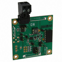
ORDERING INFORMATION1 Device NCP5050MTTXG †For information on tape and reel specifications, including part orientation and tape sizes, please refer to our Tape and Reel Packaging Specification Brochure, BRD8011/D. Demo Board Available: • The NCP5050EVB/D evaluation board that configures the device ...

Page 14

... B 0.3008 NOTE 3 0.05 C *For additional information on our Pb−Free strategy and soldering details, please download the ON Semiconductor Soldering and Mounting Techniques Reference Manual, SOLDERRM/D. N. American Technical Support: 800−282−9855 Toll Free USA/Canada Europe, Middle East and Africa Technical Support: Phone: 421 33 790 2910 Japan Customer Focus Center Phone: 81− ...

Related keywords