AS1112 EB austriamicrosystems, AS1112 EB Datasheet - Page 10
AS1112 EB
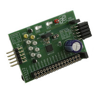
Manufacturer Part Number
AS1112 EB
Description
BOARD EVAL AS1112
Manufacturer
austriamicrosystems
Specifications of AS1112 EB
Current - Output / Channel
0.5 ~ 100 mA
Outputs And Type
16, Non-Isolated
Voltage - Output
0 ~ 15 V
Features
Over-Temperature, Open-LED, Shorted-LED, Diagnostics
Voltage - Input
3 ~ 5.5 V
Utilized Ic / Part
AS1112
Lead Free Status / RoHS Status
Lead free by exemption / RoHS compliant by exemption


AS1112
Datasheet - D e t a i l e d D e s c r i p t i o n
Figure 8. Error Detection Timing (GS=FFFF
Note: The rising edge of LD latches new data into the internal registers depending on the logic level of the pin MODE. If the pin MODE is tied
Delay Between Outputs (only for AS1112 and AS1112B)
The AS1112 uses graduated delay circuits between OUTn outputs. These circuits are contained in the constant-current driver block of the
AS1112
The maximum delay is 450ns (typ) from OUT0 to OUT15. The delay scheme works by switching on and switching off each output channel. Thus
the on/off time of each channel is the same regardless of the delay. These delays prevent large inrush currents and switching noise that can
reduce bypass capacitance when the outputs are switched on.
OUTn Enable
All OUTn channels can be collectively switched off with one signal. When OEN is set to 1, all OUTn channels are disabled, regardless of the
device logic operations. The greyscale counter is also reset when OEN is set to 1.
When OEN is set to 0, all OUTn channels are in normal operation.
Table 9. Pin OEN Truth Table
Setting Maximum Channel Current
The maximum output current per channel is programmed by a single resistor, R
on pin I
multiplied by a factor of 31.5. The maximum output current is calculated as:
Where:
V
R
Figure 5 on page 7
GND, and I
www.austriamicrosystems.com/LED-Driver-ICs/AS1112
IREF
IREF
= 1.24V;
= User-selected external resistor.
REF
(see Figure 1 on page
GND, the greyscale registers are updated. If the pin MODE is tied to V
OEN
OUT
is set by an internal band gap V
0
1
is the constant output current of OUT0:OUT15.
shows the maximum output current I
GSCLK
OEN
SID
LD
1). The average-delay time is 30ns (typ).
Normal Operation
OUT0:OUT15
Disabled
IREF
HEX
, DC=3F
(1.24V typ). The maximum channel current is equivalent to the current flowing through R
Detection
Error
Start
OUT
HEX
I
MAX
)
versus R
=
Revision 1.09
LODn, LSDn
R
V
IREF
IREF
IREF
, where R
>1µs
x 31.5
IREF
CC
, the dot correction registers are updated.
, which is placed between pin I
IREF
is the value of the resistor between I
Detection
LODn+1, LSDn+1
Error
End
REF
and GND. The voltage
REF
terminal to
(EQ 1)
10 - 19
IREF
Related parts for AS1112 EB
Image
Part Number
Description
Manufacturer
Datasheet
Request
R

Part Number:
Description:
IC DRIVER LED 16-CHAN 32-TQFN
Manufacturer:
austriamicrosystems
Datasheet:

Part Number:
Description:
16-Channel LED Driver
Manufacturer:
austriamicrosystems AG
Datasheet:
Part Number:
Description:
IC SWITCH QUAD SPST 14-TSSOP
Manufacturer:
austriamicrosystems
Datasheet:
Part Number:
Description:
IC SWITCH QUAD SPST 14-TSSOP
Manufacturer:
austriamicrosystems
Datasheet:
Part Number:
Description:
IC AMP AUDIO MONO 1.8W 10-MSOP
Manufacturer:
austriamicrosystems
Datasheet:
Part Number:
Description:
IC AMP AUDIO MONO 1.8W 10-MSOP
Manufacturer:
austriamicrosystems
Datasheet:
Part Number:
Description:
IC AMP AUDIO MONO 1.8W 10-MSOP
Manufacturer:
austriamicrosystems
Datasheet:
Part Number:
Description:
IC AMP AUD 1.8W 3DB GAIN 10-MSOP
Manufacturer:
austriamicrosystems
Datasheet:
Part Number:
Description:
IC DRIVER LED 8-DIGIT 24-SOIC
Manufacturer:
austriamicrosystems
Datasheet:
Part Number:
Description:
IC DRIVER LED 8-DIGIT 24-SOIC
Manufacturer:
austriamicrosystems
Datasheet:
Part Number:
Description:
IC, LINE/SPEAKER PHONE CIRCUIT, SOIC-28
Manufacturer:
austriamicrosystems
Datasheet:
Part Number:
Description:
IC MULTI-STANDARD CMOS TELEPHONE SOIC-28
Manufacturer:
austriamicrosystems
Datasheet:
Part Number:
Description:
IC MULTI-STANDARD CMOS TELEPHONE SOIC-28
Manufacturer:
austriamicrosystems
Datasheet:
Part Number:
Description:
IC MULTI-STANDARD CMOS TELEPHONE SOIC-28
Manufacturer:
austriamicrosystems
Datasheet:
Part Number:
Description:
CABGA 64 (7x7)
Manufacturer:
austriamicrosystems
Datasheet: