SOT89-3EV-VREG Microchip Technology, SOT89-3EV-VREG Datasheet - Page 4
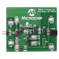
SOT89-3EV-VREG
Manufacturer Part Number
SOT89-3EV-VREG
Description
BOARD EVAL SOT89-3 VOLTAGE REG
Manufacturer
Microchip Technology
Datasheets
1.SOT89-3EV-VREG.pdf
(24 pages)
2.SOT89-3EV-VREG.pdf
(26 pages)
3.SOT89-3EV-VREG.pdf
(28 pages)
4.SOT89-3EV-VREG.pdf
(22 pages)
5.SOT89-3EV-VREG.pdf
(22 pages)
Specifications of SOT89-3EV-VREG
Channels Per Ic
1 - Single
Regulator Type
Positive Fixed
Board Type
Partially Populated
Utilized Ic / Part
SOT-89-3 Package
Silicon Manufacturer
Microchip
Application Sub Type
Voltage Regulator
Kit Application Type
Power Management - Voltage Regulator
Silicon Core Number
MCP1700A, MCP1701A, MCP1702, MCP1703
Lead Free Status / RoHS Status
Lead free / RoHS Compliant
Current - Output
-
Voltage - Output
-
Voltage - Input
-
Operating Temperature
-
Lead Free Status / Rohs Status
Lead free / RoHS Compliant


MCP1702
DC CHARACTERISTICS (CONTINUED)
DS22008E-page 4
Electrical Specifications: Unless otherwise specified, all limits are established for V
I
Boldface type applies for junction temperatures, T
Dropout Voltage
(Note
Output Delay Time
Output Noise
Power Supply Ripple
Rejection Ratio
Thermal Shutdown
Protection
Note 1:
LOAD
= 100 µA, C
1,
2:
3:
4:
5:
6:
7:
Parameters
Note
The minimum V
V
input voltage V
TCV
temperature range. V
Load regulation is measured at a constant junction temperature using low duty cycle pulse testing. Changes in output
voltage due to heating effects are determined using thermal regulation specification TCV
Dropout voltage is defined as the input to output differential at which the output voltage drops 2% below its measured
value with an applied input voltage of V
The maximum allowable power dissipation is a function of ambient temperature, the maximum allowable junction
temperature and the thermal resistance from junction to air (i.e., T
dissipation will cause the device operating junction temperature to exceed the maximum 150°C rating. Sustained
junction temperatures above 150°C can impact the device reliability.
The junction temperature is approximated by soaking the device under test at an ambient temperature equal to the
desired Junction temperature. The test time is small enough such that the rise in the Junction temperature over the
ambient temperature is not significant.
R
5)
is the nominal regulator output voltage. For example: V
OUT
OUT
= (V
= 1 µF (X7R), C
OUT-HIGH
IN
IN
= V
must meet two conditions: V
V
OUT(MAX)
DROPOUT
T
OUT-LOW
PSRR
- V
Sym
DELAY
T
e
SD
N
OUT-LOW
IN
= 1 µF (X7R), T
+ V
= lowest voltage measured over the temperature range.
DROPOUT(MAX)
) *10
Min
—
—
—
—
—
—
—
—
—
J
6
OUT(MAX)
of -40°C to +125°C.
/ (V
R
A
* Temperature), V
= +25°C.
IN
1000
Typ
330
525
625
750
150
2.7V and V
44
or V
+ V
—
8
DROPOUT(MAX)
IN
= 2.7V (whichever is greater); I
R
1100
Max
= 1.2V, 1.5V, 1.8V, 2.5V, 2.8V, 3.0V, 3.3V, 4.0V, or 5.0V. The
650
725
975
(Note
—
—
—
—
—
IN
V
OUT-HIGH
A
7)
, T
or 2.7V, whichever is greater.
OUT(MAX)
µV/(Hz)
J
,
Units
mV
mV
mV
mV
mV
IN
dB
JA
µs
°C
= highest voltage measured over the
= V
). Exceeding the maximum allowable power
1/2
+ V
OUT(MAX)
I
I
I
I
V
Current Parameter
V
R
I
f = 100 Hz, C
V
V
DROPOUT(MAX)
L
L
L
L
L
R
IN
INAC
R
L
= 250 mA, V
= 250 mA, 3.3V V
= 250 mA, 2.8V V
= 250 mA, 2.5V V
= 50 mA, f = 1 kHz, C
= 50 resistive
< 2.5V, See Maximum Output
= 1.2V
2010 Microchip Technology Inc.
= 0V to 6V, V
OUT
= 100 mV pk-pk, C
+ V
OUT
= 100 µA.
DROPOUT(MAX)
.
Conditions
OUT
.
R
= 5.0V
OUT
= 1 µF, I
= 90% V
R
R
R
< 5.0V
< 3.3V
< 2.8V
OUT
,
IN
Note
L
= 50 mA,
= 0 µF,
= 1 µF
R
1,
Related parts for SOT89-3EV-VREG
Image
Part Number
Description
Manufacturer
Datasheet
Request
R

Part Number:
Description:
Manufacturer:
Infineon Technologies
Datasheet:
Part Number:
Description:
Manufacturer:
Infineon Technologies
Datasheet:
Part Number:
Description:
Manufacturer:
Infineon Technologies
Datasheet:
Part Number:
Description:
Manufacturer:
Infineon Technologies
Datasheet:
Part Number:
Description:
Manufacturer:
Infineon Technologies
Datasheet:
Part Number:
Description:
Manufacturer:
Infineon Technologies
Datasheet:
Part Number:
Description:
Manufacturer:
Infineon Technologies
Datasheet:
Part Number:
Description:
Manufacturer:
Infineon Technologies
Datasheet:
Part Number:
Description:
Manufacturer:
Infineon Technologies
Datasheet:
Part Number:
Description:
Manufacturer:
Infineon Technologies
Datasheet:
Part Number:
Description:
Manufacturer:
Infineon Technologies
Datasheet:
Part Number:
Description:
Manufacturer:
Infineon Technologies
Datasheet: