SOT89-3EV-VREG Microchip Technology, SOT89-3EV-VREG Datasheet - Page 9
SOT89-3EV-VREG
Manufacturer Part Number
SOT89-3EV-VREG
Description
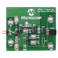
BOARD EVAL SOT89-3 VOLTAGE REG
Manufacturer
Microchip Technology
Datasheets
1.SOT89-3EV-VREG.pdf
(24 pages)
2.SOT89-3EV-VREG.pdf
(26 pages)
3.SOT89-3EV-VREG.pdf
(28 pages)
4.SOT89-3EV-VREG.pdf
(22 pages)
5.SOT89-3EV-VREG.pdf
(22 pages)
Specifications of SOT89-3EV-VREG
Channels Per Ic
1 - Single
Regulator Type
Positive Fixed
Board Type
Partially Populated
Utilized Ic / Part
SOT-89-3 Package
Silicon Manufacturer
Microchip
Application Sub Type
Voltage Regulator
Kit Application Type
Power Management - Voltage Regulator
Silicon Core Number
MCP1700A, MCP1701A, MCP1702, MCP1703
Lead Free Status / RoHS Status
Lead free / RoHS Compliant
Current - Output
-
Voltage - Output
-
Voltage - Input
-
Operating Temperature
-
Lead Free Status / Rohs Status
Lead free / RoHS Compliant


3.0
The descriptions of the pins are listed in
TABLE 3-1:
3.1
Regulator ground. Tie GND to the negative side of the
output and the negative side of the input capacitor.
Only the LDO bias current (2 µA, typ.) flows out of this
pin, there is no high current. The LDO output regulation
is referenced to this pin. Minimize voltage drops
between this pin and the negative side of the load.
3.2
Connect V
positive terminal of the output capacitor. The positive
side of the output capacitor should be physically
located as close as possible to the LDO V
current flowing out of this pin is equal to the DC load
current.
© 2007 Microchip Technology Inc.
SOT-23A
Pin No.
1
2
3
PIN DESCRIPTIONS
Ground Terminal (GND)
Regulated Voltage Output (V
OUT
to the positive side of the load and the
Pin No.
SOT-89
PIN FUNCTION TABLE
1
3
2
Pin No.
TO-92
1
3
2
Table
OUT
pin. The
OUT
3-1.
Name
V
GND
V
OUT
IN
)
Ground Terminal
Regulated Voltage Output
Unregulated Supply Input
3.3
Connect the input supply voltage and the positive side
of the input capacitor to V
regulators, low source impedance is necessary for the
stable operation of the LDO. The amount of
capacitance required to ensure low source impedance
will depend on the proximity of the input source
capacitors or battery type. The input capacitor should
be physically located as close as possible to the V
pin. For most applications, 1 µF of capacitance will
ensure stable operation of the LDO circuit. For
applications that have load currents below 100 mA, the
input capacitance requirement can be lowered. The
type of capacitor used can be ceramic, tantalum or
aluminum electrolytic. The low equivalent series
resistance characteristics of the ceramic will yield
better noise and PSRR performance at high frequency.
The current flow into this pin is equal to the DC load
current, plus the LDO bias current (2 µA, typical).
Unregulated Supply Input (V
Function
IN
MCP1701A
. Like all low-dropout linear
DS21991C-page 9
IN
)
IN
Related parts for SOT89-3EV-VREG
Image
Part Number
Description
Manufacturer
Datasheet
Request
R

Part Number:
Description:
Manufacturer:
Infineon Technologies
Datasheet:
Part Number:
Description:
Manufacturer:
Infineon Technologies
Datasheet:
Part Number:
Description:
Manufacturer:
Infineon Technologies
Datasheet:
Part Number:
Description:
Manufacturer:
Infineon Technologies
Datasheet:
Part Number:
Description:
Manufacturer:
Infineon Technologies
Datasheet:
Part Number:
Description:
Manufacturer:
Infineon Technologies
Datasheet:
Part Number:
Description:
Manufacturer:
Infineon Technologies
Datasheet:
Part Number:
Description:
Manufacturer:
Infineon Technologies
Datasheet:
Part Number:
Description:
Manufacturer:
Infineon Technologies
Datasheet:
Part Number:
Description:
Manufacturer:
Infineon Technologies
Datasheet:
Part Number:
Description:
Manufacturer:
Infineon Technologies
Datasheet:
Part Number:
Description:
Manufacturer:
Infineon Technologies
Datasheet: