AD8330-EVALZ Analog Devices Inc, AD8330-EVALZ Datasheet

BOARD EVAL FOR AD8330

AD8330-EVALZ

Manufacturer Part Number
AD8330-EVALZ
Description
BOARD EVAL FOR AD8330
Manufacturer
Analog Devices Inc
Datasheets

Specifications of AD8330-EVALZ

Channels Per Ic
1 - Single
Amplifier Type
Variable Gain
Output Type
Differential, Rail-to-Rail
Slew Rate
1500 V/µs
-3db Bandwidth
150MHz
Operating Temperature
-40°C ~ 85°C
Current - Supply (main Ic)
20mA
Voltage - Supply, Single/dual (±)
2.7 V ~ 6 V
Board Type
Fully Populated
Utilized Ic / Part
AD8330
Silicon Manufacturer
Analog Devices
Application Sub Type
Variable Gain Amplifier
Kit Application Type
Amplifier
Silicon Core Number
AD8330
Kit Contents
Board
Lead Free Status / RoHS Status
Lead free / RoHS Compliant
Current - Output / Channel
-
Lead Free Status / RoHS Status
Lead free / RoHS Compliant, Lead free / RoHS Compliant
GENERAL DESCRIPTION
The EVAL-AD8330EB is an easy-to-use accessory that enables a
hands-on evaluation of the
(VGA). It includes test pins for connections to all of the functional
device inputs. Figure 1 is a full size photograph of the board.
Rev. B
Information furnished by Analog Devices is believed to be accurate and reliable. However, no
responsibility is assumed by Analog Devices for its use, nor for any infringements of patents or other
rights of third parties that may result from its use. Specifications subject to change without notice. No
license is granted by implication or otherwise under any patent or patent rights of Analog Devices.
Trademarks and registered trademarks are the property of their respective owners.
Figure 1. Photograph of the AD8330 Evaluation Board
IN
R5
49.9Ω
–5V
AD8330
0.1μF
C18
+
AD8131
variable gain amplifier
24.9Ω
C17
10μF
10V
0.1μF
0.1μF
10μF
R13
10V
C20
C15
C1
+5V
+
8
2
1
+5V
3
6
4
AGND
5
AGND
VDBS
C14
0.01μF
C16
0.01μF
0.1μF
0.1μF
C5
C3
0.1μF
Figure 2. Schematic Diagram
C6
IN_HI/LO
OFST
DOWN
R1
W2
+5V
W4
0.1μF
C2
CMGN1
ENB
W3
UP
1
2
3
4
5
6
7
8
One Technology Way, P.O. Box 9106, Norwood, MA 02062-9106, U.S.A.
Tel: 781.329.4700
Fax: 781.461.3113
BASIC OPERATION
The input SMA connector IN is terminated with a 49.9 Ω
resistor (see Figure 2). For convenience, the board includes an
AD8131
ended signal source to the differential input of the AD8330. If
desired, the AD8131 can be removed and the AD8330 can be
driven at one of its inputs from a single-ended source.
The AD8330 output is observed at the SMA connectors OUT_HI
and OUT_LO or by using the 2-pin header OUT_HI/ OUT_LO
adjacent to the device.
The AD8330 requires only a +5 V power supply; however, because
of the AD8131 buffer bipolar power supply requirements, ±5 V
supplies are required to power the board. The current required
for the board is approximately 40 mA from the +5 V supply and
10 mA from the −5 V supply.
OPTIONS
Table 1 lists the jumpers on the board and their functions.
Consult the
functions.
FLTR
OFST
ENBL
VPSI
INHI
INLO
MODE
VDBS
CMGN
W1
AD8330
C13
1nF
COMM
CMOP
VMAG
VPOS
CNTR
VPSO
OPLO
OPHI
high speed differential amplifier to convert a single-
AD8330 Evaluation Board
AD8330
R12
1kΩ
16
15
14
13
12
11
10
9
C12
0.1μF
C19
0.1μF
C11
0.1μF
VCMD
data sheet for further explanation of their
C9
12pF
C8
12pF
+5V
0.1μF
©2006 Analog Devices, Inc. All rights reserved.
C7
AGND
+5V
OUT_HI/LO
EVAL-AD8330EB
0.1μF
0.1μF
C10
C4
VMAG
AGND
OUT_LO
OUT_HI
www.analog.com

Related parts for AD8330-EVALZ

AD8330-EVALZ Summary of contents

Page 1

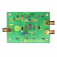
... Figure 2). For convenience, the board includes an AD8131 ended signal source to the differential input of the AD8330. If desired, the AD8131 can be removed and the AD8330 can be driven at one of its inputs from a single-ended source. The AD8330 output is observed at the SMA connectors OUT_HI and OUT_LO or by using the 2-pin header OUT_HI/ OUT_LO adjacent to the device ...

Page 2

... OUT_HI and OUT_LO can also be used, but the user may need to account for load capacitance effects. EVAL-AD8330EB BOARD DESIGN The EVAL-AD8330EB is a 4-layer design for maximum ground- plane area. The evaluation board side silkscreen and wiring patterns are shown in Figure 4 through Figure 9. ...

Page 3

... Figure 4. Component-Side Silkscreen Figure 5. Component-Side Wiring Figure 6. Inner Layer 1 Figure 7. Wiring-Side Silkscreen Figure 8. Wiring-Side Pattern Figure 9. Inner Layer 2 Rev Page EVAL-AD8330EB ...

Page 4

... EVAL-AD8330EB Table 2. AD8330 Parts List Pin No. Quantity Description 1 1 Resistor SM, 49.9 Ω, 1%, 1/16 W, 0603 2 1 Resistor SM, 24.9 Ω, 1%, 1/8 W, 1206 3 1 Resistor SM, 0 Ω, 5%, 1/8 W, 1206 4 1 Resistor SM, 1 kΩ, 1%, 1/8 W, 1206 5 11 Capacitor SM, 0.1 μ 1206 6 2 Capacitor SM, 0.1 μ 0603 ...

Related keywords