LMP8601MAEVAL/NOPB National Semiconductor, LMP8601MAEVAL/NOPB Datasheet - Page 4
LMP8601MAEVAL/NOPB
Manufacturer Part Number
LMP8601MAEVAL/NOPB
Description
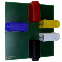
BOARD EVALUATION FOR LMP8601MA
Manufacturer
National Semiconductor
Series
LMP®r
Specifications of LMP8601MAEVAL/NOPB
Channels Per Ic
1 - Single
Amplifier Type
Current Sense
Output Type
Single-Ended
Slew Rate
0.83 V/µs
Current - Output / Channel
48mA
Operating Temperature
-40°C ~ 125°C
Current - Supply (main Ic)
1.1mA
Voltage - Supply, Single/dual (±)
3 V ~ 5.5 V
Board Type
Fully Populated
Utilized Ic / Part
LMP8601
Silicon Manufacturer
National
Silicon Core Number
LMP8601, LMP8601Q
Kit Application Type
Amplifier
Application Sub Type
Current-Sense Amplifier
Kit Contents
Board, Doc
Lead Free Status / RoHS Status
Lead free / RoHS Compliant
-3db Bandwidth
-
Other names
LMP8601MAEVAL


www.national.com
Output Buffer (From A2 (pin 4) to OUT( pin 5 ))
V
A2
I
A2 V
I
B
SC
Symbol
OS
Note 1: “Absolute Maximum Ratings” indicate limits beyond which damage to the device may occur, including inoperability and degradation of the device reliability
and/or performance. Functional operation of the device and/or non-degradation at the Absolute Maximum Ratings or other conditions beyond those indicated in
the Recommended Operating Conditions is not implied. The Recommended Operating Conditions indicate conditions at which the device is functional and the
device should not be beyond such conditions. All voltages are measured with respect to the ground pin, unless otherwise specified.
Note 2: The electrical Characteristics tables list guaranteed specifications under the listed Recommended Operating Conditions except as otherwise modified or
specified by the Electrical Characteristics Conditions and/or Notes. Typical specifications are estimations only and are not guaranteed.
Note 3: The maximum power dissipation must be derated at elevated temperatures and is dictated by T
allowable power dissipation P
Note 4: Human Body Model per MIL-STD-883, Method 3015.7. Machine Model, per JESD22-A115-A. Field-Induced Charge-Device Model, per JESD22-C101-
C.
Note 5: Typical values represent the most likely parameter norms at T
characterization and are not guaranteed.
Note 6: Datasheet min/max specification limits are guaranteed by test.
Note 7: Slew rate is the average of the rising and falling slew rates.
Note 8: Offset voltage drift determined by dividing the change in V
Note 9: AC Common Mode Signal is a 5V
Note 10: Positive current corresponds to current flowing into the device
Note 11: For this test input is driven from A1 stage.
Note 12: For V
Note 13: Short-Circuit test is a momentary test. Continuous short circuit operation at elevated ambient temperature can result in exceeding the maximum allowed
junction temperature of 150°C
Note 14: Both the gain of the preamplifier A1
measured to assure the gain of all parts is always within the A
V
OUT
Input Offset Voltage
Gain
Input Bias Current of A2
A2 Ouput Voltage Swing
(Note
Output Short-Circuit Current
OL
, R
(Note
11,
L
is connected to V
Note
14)
DMAX
Parameter
12)
= (T
J(MAX)
S
and for V
PP
(Note
sine-wave (0V to 5V) at the given frequency.
- T
V
and the gain of the buffer amplifier A2
A
(Note
)/ θ
OH
10)
JA
, R
or the number given in Absolute Maximum Ratings, whichever is lower.
L
13)
is connected to GND.
V
limits
0V
V
V
Sourcing, V
Sinking, V
OS
OL
OH
at temperature extremes into the total temperature change.
≤
A
= +25°C, and at the Recommended Operation Conditions at the time of product
V
CM
IN
≤
4
IN
Conditions
V
= GND, V
S
= V
V
are measured individually. The over all gain of both amplifiers A
S
, V
OUT
R
OUT
L
= 100 kΩ
= GND
= V
J(MAX)
S
, θ
JA
, and the ambient temperature, T
(Note
−2.5
1.99
4.98
Min
–25
−2
30
6)
(Note
±0.5
4.99
Typ
−40
–42
48
2
4
5)
(Note
Max
2.01
±20
–60
2.5
20
65
2
A
. The maximum
6)
V
is also
Units
mV
V/V
mV
mA
nA
fA
V
Related parts for LMP8601MAEVAL/NOPB
Image
Part Number
Description
Manufacturer
Datasheet
Request
R

Part Number:
Description:
National Semiconductor [8-Bit D/A Converter]
Manufacturer:
National Semiconductor
Datasheet:
Part Number:
Description:
National Semiconductor [Media Coprocessor]
Manufacturer:
National Semiconductor
Datasheet:
Part Number:
Description:
Digitally Controlled Tone and Volume Circuit with Stereo Audio Power Amplifier, Microphone Preamp Stage and National 3D Sound
Manufacturer:
National Semiconductor
Datasheet:
Part Number:
Description:
Digitally Controlled Tone and Volume Circuit with Stereo Audio Power Amplifier, Microphone Preamp Stage and National 3D Sound
Manufacturer:
National Semiconductor
Datasheet:
Part Number:
Description:
AC97 Rev 2 Codec with Sample Rate Conversion and National 3D Sound
Manufacturer:
National Semiconductor
Part Number:
Description:
Manufacturer:
National Semiconductor
Datasheet:
Part Number:
Description:
Manufacturer:
National Semiconductor
Datasheet:
Part Number:
Description:
General Purpose, Low Voltage, Low Power, Rail-to-Rail Output Operational Amplifiers
Manufacturer:
National Semiconductor
Datasheet:
Part Number:
Description:
8-bit 20 MSPS flash A/D converter.
Manufacturer:
National Semiconductor
Datasheet:
Part Number:
Description:
Low Noise Quad Operational Amplifier
Manufacturer:
National Semiconductor
Datasheet:
Part Number:
Description:
Quad Differential Line Receivers
Manufacturer:
National Semiconductor
Datasheet:
Part Number:
Description:
Quad High Speed Trapezoidal? Bus Transceiver
Manufacturer:
National Semiconductor
Datasheet:
Part Number:
Description:
Dual Line Receiver
Manufacturer:
National Semiconductor
Datasheet:
Part Number:
Description:
TTL to 10k ECL Level Translator with Latch
Manufacturer:
National Semiconductor
Datasheet: