MCP6V01DM-VOS Microchip Technology, MCP6V01DM-VOS Datasheet - Page 5
MCP6V01DM-VOS
Manufacturer Part Number
MCP6V01DM-VOS
Description
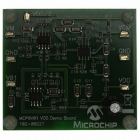
DEMO BOARD FOR MCP6V01
Manufacturer
Microchip Technology
Specifications of MCP6V01DM-VOS
Channels Per Ic
1 - Single
Amplifier Type
Chopper (Zero-Drift)
Output Type
Rail-to-Rail
Slew Rate
0.5 V/µs
Current - Output / Channel
22mA
Operating Temperature
-40°C ~ 125°C
Voltage - Supply, Single/dual (±)
1.8 V ~ 5.5 V
Board Type
Fully Populated
Utilized Ic / Part
MCP6V01
Silicon Manufacturer
Microchip
Application Sub Type
Operational Amplifier
Kit Application Type
Amplifier
Silicon Core Number
MCP6V01, MCP6V03, MCP6V06, MCP6V08
Kit Contents
Board
Lead Free Status / RoHS Status
Lead free / RoHS Compliant
-3db Bandwidth
-
Current - Supply (main Ic)
-
Lead Free Status / Rohs Status
Lead free / RoHS Compliant


INTRODUCTION
DOCUMENT LAYOUT
© 2009 Microchip Technology Inc.
All documentation becomes dated, and this manual is no exception. Microchip tools and
documentation are constantly evolving to meet customer needs, so some actual dialogs
and/or tool descriptions may differ from those in this document. Please refer to our web site
(www.microchip.com) to obtain the latest documentation available.
Documents are identified with a “DS” number. This number is located on the bottom of each
page, in front of the page number. The numbering convention for the DS number is
“DSXXXXXA”, where “XXXXX” is the document number and “A” is the revision level of the
document.
For the most up-to-date information on development tools, see the MPLAB
Select the Help menu, and then Topics to open a list of available on-line help files.
This chapter contains general information that will be useful to know before using the
MCP6V01 Input Offset Demo Board. Items discussed in this chapter include:
• Document Layout
• Conventions Used in this Guide
• Recommended Reading
• The Microchip Web Site
• Customer Support
• Document Revision History
This document describes how to use the MCP6V01 Input Offset Demo Board. The
manual layout is as follows:
• Chapter 1. “Product Overview” - Important information about the MCP6V01
• Chapter 2. “Installation and Operation” – Covers the initial set-up of the
• Chapter 3. “Possible Modifications” - Shows simple modifications to the
• Appendix A. “Schematics and Layouts” – Shows the schematic and board
• Appendix B. “Bill Of Materials (BOM)” – Lists the parts used to build the
Input Offset Demo Board.
MCP6V01 Input Offset Demo Board. It lists the required tools and shows how to
connect and set up the lab equipment. The basic theory on converting
measurements to offset voltage, open-loop gain, CMRR, PSRR and input offset
drift is given, along with a worked example. Hints are then given on reducing
measurement noise.
MCP6V01 Input Offset Demo Board.
layouts for the MCP6V01 Input Offset Demo Board.
sub-assemblies in the MCP6V01 Input Offset Demo Board.
NOTICE TO CUSTOMERS
Preface
DEMO BOARD USER’S GUIDE
MCP6V01 INPUT OFFSET
®
IDE on-line help.
DS51801A-page 1
Related parts for MCP6V01DM-VOS
Image
Part Number
Description
Manufacturer
Datasheet
Request
R

Part Number:
Description:
IC OPAMP AUTO-ZERO SNGL 8SOIC
Manufacturer:
Microchip Technology
Datasheet:

Part Number:
Description:
300 ?A, Auto-Zeroed Op Amps
Manufacturer:
MICROCHIP [Microchip Technology]
Datasheet:
Part Number:
Description:
Op Amps Sngl Auto-Zero Op Amp E temp
Manufacturer:
Microchip Technology

Part Number:
Description:
300 ?a, Auto-zeroed Op Amps
Manufacturer:
Microchip Technology Inc.
Datasheet:
Part Number:
Description:
Manufacturer:
Microchip Technology Inc.
Datasheet:
Part Number:
Description:
Manufacturer:
Microchip Technology Inc.
Datasheet:
Part Number:
Description:
Manufacturer:
Microchip Technology Inc.
Datasheet:
Part Number:
Description:
Manufacturer:
Microchip Technology Inc.
Datasheet:
Part Number:
Description:
Manufacturer:
Microchip Technology Inc.
Datasheet:
Part Number:
Description:
Manufacturer:
Microchip Technology Inc.
Datasheet:
Part Number:
Description:
Manufacturer:
Microchip Technology Inc.
Datasheet: