MCP651EV-VOS Microchip Technology, MCP651EV-VOS Datasheet - Page 6
MCP651EV-VOS
Manufacturer Part Number
MCP651EV-VOS
Description
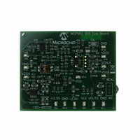
BOARD EVAL OP AMP MCP651
Manufacturer
Microchip Technology
Series
mCal Technologyr
Specifications of MCP651EV-VOS
Channels Per Ic
1 - Single
Amplifier Type
General Purpose
Output Type
Single-Ended, Rail-to-Rail
Slew Rate
30 V/µs
Current - Output / Channel
100mA
Operating Temperature
-40°C ~ 125°C
Current - Supply (main Ic)
6mA
Voltage - Supply, Single/dual (±)
2.5 V ~ 5.5 V
Board Type
Fully Populated
Utilized Ic / Part
MCP651
Processor To Be Evaluated
MCP651
Maximum Operating Temperature
+ 125 C
Minimum Operating Temperature
- 40 C
Operating Supply Voltage
2.5 V to 5.5 V
Tool Type
Evaluation Board
Core Architecture
PIC
Cpu Core
PIC
Data Bus Width
8 bit
Lead Free Status / RoHS Status
Lead free / RoHS Compliant
-3db Bandwidth
-
Lead Free Status / Rohs Status
Lead free / RoHS Compliant
Available stocks
Company
Part Number
Manufacturer
Quantity
Price
Company:

Part Number:
MCP651EV-VOS
Manufacturer:
Microchip Technology
Quantity:
135
Company:
Part Number:
MCP651EV-VOS
Manufacturer:
MICROCHIP
Quantity:
12 000


MCP6V01/2/3
1.3
FIGURE 1-1:
FIGURE 1-2:
Time.
FIGURE 1-3:
FIGURE 1-4:
DS22058C-page 6
V
V
OUT
V
V
V
I
CS
I
I
V
OUT
DD
SS
CS
V
OS
DD
OS
IN
IN
1 µA
(typical)
-2 µA
(typical)
V
(typical)
Timing Diagrams
V
0V
DD
DD
High-Z
/5 MΩ
t
t
ODR
ON
1.8V
t
V
t
STL
STR
IL
Amplifier Start Up.
Offset Correction Settling
Output Overdrive Recovery.
Chip Select (MCP6V03).
V
DD
(typical)
(typical)
(typical)
300 µA
300 µA
/2
5 pA
V
SS
V
t
ODR
IH
1.8V to 5.5V
V
V
V
V
OS
OS
OS
OS
t
OFF
V
+ 50 µV
– 50 µV
+ 50 µV
+ 50 µV
DD
(typical)
(typical)
(typical)
High-Z
/5 MΩ
-2 µA
1 µA
1.4
The circuits used for the DC and AC tests are shown in
Figure 1-5
out as discussed in Section 4.3.8 “Supply Bypassing
and Filtering”. R
of R
FIGURE 1-5:
Most Non-Inverting Gain Conditions.
FIGURE 1-6:
Most Inverting Gain Conditions.
The circuit in
dynamic behavior (i.e., IMD, t
potentiometer balances the resistor network (V
should equal V
mode input voltage is V
input (V
10 V/V.
FIGURE 1-7:
Input Behavior.
V
V
V
V
V
DD
DD
IN
F
IN
IN
MCP6V0X
MCP6V0X
and R
/3
/3
20.0 kΩ
20.0 kΩ
ERR
0.1%
0.1%
Test Circuits
R
R
R
R
N
G
N
G
and
G
) appears at V
to minimize bias current effects.
Figure
Figure 1-7
REF
20.0 kΩ
MCP6V0X
20.0 kΩ
N
0.1%
0.1%
V
V
V
DD
DD
DD
is equal to the parallel combination
at DC). The op amp’s common
AC and DC Test Circuit for
AC and DC Test Circuit for
Test Circuit for Dynamic
100 nF
100 nF
100 nF
1-6. Lay the bypass capacitors
1 µF
© 2008 Microchip Technology Inc.
CM
R
R
25 turn
24.9 Ω
1 µF
1 µF
50Ω
F
F
tests the op amp input’s
OUT
= V
STR
IN
R
R
with a noise gain of
, t
/2. The error at the
ISO
ISO
R
STL
C
C
ISO
L
L
C
and t
L
V
REF
R
R
L
L
ODR
V
V
V
L
L
L
V
V
V
R
). The
OUT
OUT
OUT
L
OUT
Related parts for MCP651EV-VOS
Image
Part Number
Description
Manufacturer
Datasheet
Request
R

Part Number:
Description:
Manufacturer:
Microchip Technology Inc.
Datasheet:
Part Number:
Description:
Manufacturer:
Microchip Technology Inc.
Datasheet:
Part Number:
Description:
Manufacturer:
Microchip Technology Inc.
Datasheet:
Part Number:
Description:
Manufacturer:
Microchip Technology Inc.
Datasheet:
Part Number:
Description:
Manufacturer:
Microchip Technology Inc.
Datasheet:
Part Number:
Description:
Manufacturer:
Microchip Technology Inc.
Datasheet:
Part Number:
Description:
Manufacturer:
Microchip Technology Inc.
Datasheet:
Part Number:
Description:
Manufacturer:
Microchip Technology Inc.
Datasheet: