AD8336-EVALZ Analog Devices Inc, AD8336-EVALZ Datasheet - Page 24
AD8336-EVALZ
Manufacturer Part Number
AD8336-EVALZ
Description
BOARD EVALUATION FOR AD8336
Manufacturer
Analog Devices Inc
Series
X-AMP®r
Specifications of AD8336-EVALZ
Channels Per Ic
1 - Single
Amplifier Type
Variable Gain
Output Type
Single-Ended
Slew Rate
550 V/µs
-3db Bandwidth
115MHz
Current - Output / Channel
20mA
Operating Temperature
-55°C ~ 125°C
Current - Supply (main Ic)
28mA
Voltage - Supply, Single/dual (±)
±3 V ~ 12 V
Board Type
Fully Populated
Utilized Ic / Part
AD8336
Silicon Manufacturer
Analog Devices
Application Sub Type
Variable Gain Amplifier
Kit Application Type
Amplifier
Silicon Core Number
AD8336
Kit Contents
Board
Lead Free Status / RoHS Status
Lead free / RoHS Compliant
Available stocks
Company
Part Number
Manufacturer
Quantity
Price
Company:

Part Number:
AD8336-EVALZ
Manufacturer:
Analog Devices Inc
Quantity:
135


AD8336
EVALUATION BOARD
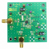
An evaluation board, AD8336-EVALZ, is available online for
the AD8336. Figure 82 is a photo of the board.
The board is shipped from the factory configured for a non-
inverting preamp gain of 4×. To change the value of the gain
of the preamp or to change the gain polarity to inverting, alter
the component values or install components in the alternate
locations provided. All components are standard 0603 size, and
the board is compliant with RoHS requirements. Table 6 shows
the components to be removed and added to change the amplifier
configuration to inverting gain.
Table 6. Component Changes for Inverting Configuration
Remove
R4, R7
OPTIONAL CIRCUITRY
The AD8336 features differential inputs for the gain control,
permitting nonzero or floating gain control inputs. To avoid any
delay in making the board operational, the gain input circuit is
shipped with Pin GNEG connected to ground via a 0 Ω resistor
in the R17 location. The user can adjust the gain of the device
by driving the GPOS test loop with a power supply or voltage
reference. Optional resistor networks R15/R17 and R13/R14
provide fixed-gain bias voltages at Pin GNEG and Pin GPOS for
non-zero common-mode voltages. The gain control can also be
driven with an active input such as a ramp. Provision is made for
an optional SMA connector at PRVG for monitoring the preamp
output or for driving the VGA from an external source. Remove
the 0 Ω resistor at R9 to isolate the preamp from an external
generator. The capacitor at Location C1 limits the bandwidth
of the preamplifier.
BOARD LAYOUT CONSIDERATIONS
The evaluation board uses four layers, with power and ground
planes located between two conductor layers. This arrangement
is highly recommended for customers, and several views of the
board are provided as reference for board layout details. When
laying out a printed circuit board for the AD8336, remember to
provide a pad beneath the device to solder the exposed pad of
the matching device. The pad in the board should have at least
five vias to provide a thermal path for the chip scale package.
Unlike leaded devices, the thermal pad is the primary means
to remove heat dissipated within the device.
Install
R5, R6
Rev. B | Page 24 of 28
Figure 82. AD8336 Evaluation Board
Figure 83. Component Side Copper
Figure 84. Secondary Side Copper
Related parts for AD8336-EVALZ
Image
Part Number
Description
Manufacturer
Datasheet
Request
R

Part Number:
Description:
±1.7g Dual-Axis IMEMS Accelerometer Evaluation Board
Manufacturer:
Analog Devices Inc
Datasheet:

Part Number:
Description:
Inertial Sensor Evaluation System
Manufacturer:
Analog Devices Inc
Datasheet:
Part Number:
Description:
Manufacturer:
Analog Devices Inc
Datasheet:
Part Number:
Description:
Manufacturer:
Analog Devices Inc
Datasheet:
Part Number:
Description:
Manufacturer:
Analog Devices Inc
Datasheet:
Part Number:
Description:
Manufacturer:
Analog Devices Inc
Datasheet:
Part Number:
Description:
Manufacturer:
Analog Devices Inc
Datasheet:
Part Number:
Description:
Manufacturer:
Analog Devices Inc
Datasheet:
Part Number:
Description:
Manufacturer:
Analog Devices Inc
Datasheet:
Part Number:
Description:
Manufacturer:
Analog Devices Inc
Datasheet:
Part Number:
Description:
Manufacturer:
Analog Devices Inc
Datasheet:
Part Number:
Description:
Manufacturer:
Analog Devices Inc
Datasheet:
Part Number:
Description:
Manufacturer:
Analog Devices Inc
Datasheet: