TMPSNS-RTD1 Microchip Technology, TMPSNS-RTD1 Datasheet - Page 17
TMPSNS-RTD1
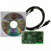
Manufacturer Part Number
TMPSNS-RTD1
Description
BOARD EVAL PT100 RTD TEMP SENSOR
Manufacturer
Microchip Technology
Datasheets
1.MCP3301-CIMS.pdf
(32 pages)
2.PCM18XR1.pdf
(438 pages)
3.MCP6S22DM-PICTL.pdf
(43 pages)
4.TMPSNS-RTD1.pdf
(26 pages)
Specifications of TMPSNS-RTD1
Sensor Type
Temperature
Interface
USB
Embedded
Yes, MCU, 8-Bit
Utilized Ic / Part
MCP3301, MCP6S26, PIC18F2550
Processor To Be Evaluated
MCP6S26, MCP3301, MCP6024, MCP41010, PIC18F2550, TC1071, MCP6002
Data Bus Width
12 bit
Interface Type
USB
Lead Free Status / RoHS Status
Not applicable / Not applicable
Voltage - Supply
-
Sensitivity
-
Sensing Range
-
Lead Free Status / RoHS Status
Lead free / RoHS Compliant, Not applicable / Not applicable


4.2.2
The input stage of the internal op amp uses two differ-
ential input stages in parallel; one operates at low V
(input voltage), while the other operates at high V
With this topology, the internal inputs can operate to
0.3V past either supply rail. The input offset voltage is
measured at both V
ensure proper operation.
The transition between the two input stages occurs
when V
linearity, avoid this region of operation.
4.2.3
The Maximum Output Voltage Swing is the maximum
swing possible under a particular output load. Accord-
ing to the specification table, the output can reach
within 60 mV of either supply rail when R
V
4.2.4
The
devices. It is designed to not exhibit phase inversion
when the input pins exceed the supply voltages.
Figure 2-34 shows an input voltage exceeding both
supplies with no resulting phase inversion.
The maximum voltage that can be applied to the input
pins (CHX) is V
inputs that exceed this absolute maximum rating can
cause excessive current to flow in or out of the input
pins. Current beyond ±2 mA can cause possible reli-
ability problems. Applications that exceed this rating
must be externally limited with an input resistor, as
shown in Figure 4-2.
FIGURE 4-2:
into an input pin.
under other conditions.
REF
2003 Microchip Technology Inc.
V
IN
= V
amplifier family is designed with CMOS input
IN
DD
R
R
IN
IN
RAIL-TO-RAIL INPUT
RAIL-TO-RAIL OUTPUT
/2. See Figure 2-21 for typical performance
INPUT VOLTAGE AND PHASE
REVERSAL
V
R
DD
------------------------------------------------------------------------------ -
SS
IN
V
--------------------------------------------------------------------------- -
Maximum expected V
- 1.5V. For the best distortion and gain
SS
- 0.3V to V
CHX
–
IN
Minimum expected V
= V
R
IN
MCP6S2X
SS
limits the current flow
2 mA
2 mA
DD
- 0.3V and V
+ 0.3V. Voltages on the
IN
–
L
V
IN
DD
= 10 k and
DD
+ 0.3V to
V
OUT
IN
IN
.
4.3
The resistor ladder shown in Figure 4-1 (R
R
with the inverting input reduces the parasitic capaci-
tance, distortion and gain mismatch.
R
causes additional current draw from the supplies.
In Shutdown mode, R
and V
fier’s inverting input are all connected through R
and the output is not high-Z (unlike the external op
amp).
While R
small. Refer to Figure 2-12.
4.4
These PGAs use a software shutdown command.
When the SPI interface sends a shutdown command,
the internal op amp is shut down and its output placed
in a high-Z state.
The resistive ladder is always connected between
V
output resistance will be on the order of 5 k and there
will be a path for output signals to appear at the input.
The Power-on Reset (POR) circuitry will temporarily
place the part in shutdown when activated. See
Section 5.4, “Power-On Reset”, for details.
REF
G
LAD
) sets the gain. Placing the gain switches in series
is an additional load on the output of the PGA and
and V
REF
LAD
Resistor Ladder
Shutdown Mode
pins. Thus, these pins and the internal ampli-
OUT
contributes to the output noise, its effect is
; even in shutdown. This means that the
MCP6S21/2/6/8
LAD
is still attached to the OUT
DS21117A-page 17
LAD
= R
LAD
F
+
Related parts for TMPSNS-RTD1
Image
Part Number
Description
Manufacturer
Datasheet
Request
R

Part Number:
Description:
Manufacturer:
Microchip Technology Inc.
Datasheet:
Part Number:
Description:
Manufacturer:
Microchip Technology Inc.
Datasheet:
Part Number:
Description:
Manufacturer:
Microchip Technology Inc.
Datasheet:
Part Number:
Description:
Manufacturer:
Microchip Technology Inc.
Datasheet:
Part Number:
Description:
Manufacturer:
Microchip Technology Inc.
Datasheet:
Part Number:
Description:
Manufacturer:
Microchip Technology Inc.
Datasheet:
Part Number:
Description:
Manufacturer:
Microchip Technology Inc.
Datasheet:
Part Number:
Description:
Manufacturer:
Microchip Technology Inc.
Datasheet: