EVAL-ADXL345Z-DB Analog Devices Inc, EVAL-ADXL345Z-DB Datasheet - Page 17
EVAL-ADXL345Z-DB
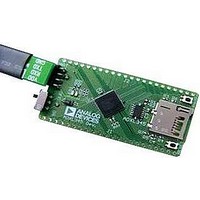
Manufacturer Part Number
EVAL-ADXL345Z-DB
Description
BOARD EVAL FOR ADXL345
Manufacturer
Analog Devices Inc
Series
iMEMS®r
Datasheets
1.EVAL-ADXL345Z.pdf
(40 pages)
2.EVAL-ADXL345Z.pdf
(2 pages)
3.EVAL-ADXL345Z.pdf
(12 pages)
Specifications of EVAL-ADXL345Z-DB
Sensor Type
Accelerometer, 3 Axis
Sensing Range
±2g, 4g, 8g, 16g
Interface
I²C, SPI
Sensitivity
256LSB/g, 128LSB/g, 64LSB/g, 32LSB/g
Voltage - Supply
2 V ~ 3.6 V
Embedded
No
Utilized Ic / Part
ADXL345
Silicon Manufacturer
Analog Devices
Application Sub Type
Accelerometer - Three-Axis
Kit Application Type
Sensing - Motion / Vibration / Shock
Silicon Core Number
ADXL345
Lead Free Status / RoHS Status
Lead free / RoHS Compliant


Table 9. SPI Digital Input/Output
Parameter
Digital Input
Low Level Input Voltage (V
High Level Input Voltage (V
Low Level Input Current (I
High Level Input Current (I
Digital Output
Low Level Output Voltage (V
High Level Output Voltage (V
Low Level Output Current (I
High Level Output Current (I
Pin Capacitance
1
Table 10. SPI Timing (T
Parameter
f
t
t
t
t
t
t
t
t
t
t
t
t
1
2
3
4
SCLK
SCLK
DELAY
QUIET
DIS
CS,DIS
S
M
SETUP
HOLD
SDO
R
F
Limits based on characterization results, not production tested.
The CS , SCLK, SDI, and SDO pins are not internally pulled up or down; they must be driven for proper operation.
Limits based on characterization results, characterized with f
The timing values are measured corresponding to the input thresholds (V
Output rise and fall times measured with capacitive load of 150 pF.
4
4
Min
200
5
5
150
0.3 × t
0.3 × t
5
5
Limit
SCLK
SCLK
A
IL
IH
IL
)
= 25°C, V
IH
OL
)
)
OH
OL
2, 3
)
OH
)
)
)
)
Max
5
10
40
20
20
S
= 2.5 V,
Unit
MHz
ns
ns
ns
ns
ns
ns
ns
ns
ns
ns
ns
ns
VDD I/O
Description
SPI clock frequency
1/(SPI clock frequency) mark-space ratio for the SCLK input is 40/60 to 60/40
CS falling edge to SCLK falling edge
SCLK rising edge to CS rising edge
CS rising edge to SDO disabled
CS deassertion between SPI communications
SCLK low pulse width (space)
SCLK high pulse width (mark)
SDI valid before SCLK rising edge
SDI valid after SCLK rising edge
SCLK falling edge to SDO/SDIO output transition
SDO/SDIO output high to output low transition
SDO/SDIO output low to output high transition
SCLK
= 1.8 V)
= 5 MHz and bus load capacitance of 100 pF; not production tested.
Test Conditions
V
V
I
I
V
V
f
OL
OH
IN
IN
IN
OL
OH
= 1 MHz, V
= 10 mA
= −4 mA
= V
= 0 V
= V
= V
Rev. B | Page 17 of 40
DD I/O
OL, max
OH, min
IL
1
and V
IN
IH
) given in Table 9.
= 2.5 V
Min
0.7 × V
−0.1
0.8 × V
10
DD I/O
DD I/O
Limit
Max
0.3 × V
0.1
0.2 × V
−4
8
1
DD I/O
DD I/O
ADXL345
Unit
V
V
μA
μA
V
V
mA
mA
pF
Related parts for EVAL-ADXL345Z-DB
Image
Part Number
Description
Manufacturer
Datasheet
Request
R

Part Number:
Description:
IC, ADJ LDO REG, 1.5V TO 5V 250mA MSOP-8
Manufacturer:
Vishay
Datasheet:

Part Number:
Description:
IC, ADJ LDO REG, 1.5V TO 5V 0.6A 8-TSSOP
Manufacturer:
Vishay
Datasheet:
Part Number:
Description:
IC, ADJ LDO REG, 1.5V TO 5V 250mA MSOP-8
Manufacturer:
Vishay
Datasheet:

Part Number:
Description:
IC ADJ LDO REG 1.5V TO 5V 150mA 5-SOT-23
Manufacturer:
Vishay
Datasheet:

Part Number:
Description:
BOARD EVAL AS1324-AD
Manufacturer:
austriamicrosystems
Datasheet:
Part Number:
Description:
IC, ADJ LDO REG, 1.5V TO 5V 0.6A 8-TSSOP
Manufacturer:
Vishay
Datasheet:

Part Number:
Description:
IC, ADJ LDO REG, 1.5V TO 5V, 0.3A, MSOP8
Manufacturer:
Vishay
Datasheet:
Part Number:
Description:
IC, ADJ LDO REG, 1.5V TO 5V, 0.3A, MSOP8
Manufacturer:
Vishay
Datasheet:
Part Number:
Description:
IC, ADJ LDO REG 1.215V TO 5V 0.3A MSOP-8
Manufacturer:
Vishay
Datasheet:
Part Number:
Description:
IC, ADJ LDO REG 1.215V TO 5V 0.3A MSOP-8
Manufacturer:
Vishay
Datasheet:

Part Number:
Description:
±1.7g Dual-Axis IMEMS Accelerometer Evaluation Board
Manufacturer:
Analog Devices Inc
Datasheet:

Part Number:
Description:
IC MULTIPLIER ANALOG 8-SOIC T/R
Manufacturer:
Analog Devices Inc
Datasheet:

Part Number:
Description:
IC ANALOG MULTIPLIER 8-DIP
Manufacturer:
Analog Devices Inc
Datasheet:
Part Number:
Description:
IC ANALOG MULTIPLIER 8-SOIC
Manufacturer:
Analog Devices Inc
Datasheet:
Part Number:
Description:
IC ANALOG MULTIPLIER 8-DIP
Manufacturer:
Analog Devices Inc
Datasheet: