ADIS16265/PCBZ Analog Devices Inc, ADIS16265/PCBZ Datasheet
ADIS16265/PCBZ
Specifications of ADIS16265/PCBZ


Related parts for ADIS16265/PCBZ


ADIS16265/PCBZ Summary of contents
Page 1
FEATURES Yaw rate gyroscope with range scaling ±80°/sec, ±160°/sec, and ±320°/sec settings No external configuration required to start data collection Start-up time: 165 ms Sleep mode recovery time: 2.5 ms Factory-calibrated sensitivity and bias ADIS16265 calibration temperature range: −40°C to ...
Page 2
ADIS16260/ADIS16265 TABLE OF CONTENTS Features .............................................................................................. 1 Applications ....................................................................................... 1 General Description ......................................................................... 1 Functional Block Diagram .............................................................. 1 Revision History ............................................................................... 2 Specifications ..................................................................................... 3 Timing Specifications .................................................................. 5 Absolute Maximum Ratings ............................................................ 6 ESD Caution .................................................................................. 6 Pin ...
Page 3
SPECIFICATIONS T = −40°C to +105° 5.0 V, angular rate = 0°/sec, ±1 g, ±320°/sec range setting, unless otherwise noted Table 1. Parameter Test Conditions/Comments SENSITIVITY 1 Clockwise rotation is positive output 25°C, dynamic range = ...
Page 4
ADIS16260/ADIS16265 Parameter Test Conditions/Comments DAC OUTPUT 5 kΩ/100 pF to GND Resolution Relative Accuracy For Code 101 to Code 4095 Differential Nonlinearity Offset Error Gain Error Output Range Output Impedance Output Settling Time LOGIC INPUTS Internal 3.3 V interface Input ...
Page 5
TIMING SPECIFICATIONS T = −40°C to +85° 5.0 V, unless otherwise noted Table 2. Parameter Description f Serial clock SCLK t Data rate period DATARATE t Stall period between data STALL t Chip select to clock ...
Page 6
ADIS16260/ADIS16265 ABSOLUTE MAXIMUM RATINGS Table 3. Parameter Acceleration Any Axis, Unpowered, 0.5 ms Any Axis, Powered, 0.5 ms VCC to GND Digital Input/Output Voltage to GND Analog Inputs to GND 1 Operating Temperature Range Storage Temperature Range 1 1 Extended ...
Page 7
PIN CONFIGURATION AND FUNCTION DESCRIPTIONS Table 4. Pin Function Descriptions 1 Pin No. Mnemonic Type Description 1 SCLK I SPI Serial Clock. 2 DOUT O SPI Data Output. Clocks output on SCLK falling edge. 3 DIN I SPI Data Input. ...
Page 8
ADIS16260/ADIS16265 TYPICAL PERFORMANCE CHARACTERISTICS 1 0.1 0.01 0.001 0 Tau (Seconds) Figure 6. Gyroscope Allan Variance MEAN +1σ –1σ 100 1k Rev Page ...
Page 9
THEORY OF OPERATION The ADIS16260 and ADIS16265 integrate a MEMS gyroscope with data sampling, signal processing, and calibration functions, along with a simple user interface. This sensing system collects data autonomously and makes it available to any processor system that ...
Page 10
ADIS16260/ADIS16265 BASIC OPERATION The ADIS16260 and ADIS16265 require only power, ground, and the four SPI signals to produce data and make it available to an embedded processor. Figure 9 provides a schematic for connecting the ADIS16260 and ADIS16265 to a ...
Page 11
SPI WRITE COMMANDS Master processors write to the control registers, one byte at a time, using the bit sequence shown in Figure 11. Some configurations require writing both bytes to a register, which takes two separate 16-bit sequences, whereas others ...
Page 12
ADIS16260/ADIS16265 MEMORY MAP All unused memory locations are reserved for future use. Table 7. User Register Memory Map Flash Name Access Backup FLASH_CNT Read only Yes SUPPLY_OUT Read only No GYRO_OUT Read only No AUX_ADC Read only No TEMP_OUT Read ...
Page 13
PROCESSING SENSOR DATA Table 8 provides a summary of the output data registers, which use the bit pattern shown in Figure 14. The ND bit is equal to 1 when the register contains unread data. The EA bit is high ...
Page 14
ADIS16260/ADIS16265 Sensor Bandwidth The gyroscope signal chain has several filter stages that shape its frequency response. Figure 15 provides a block diagram of each filter stage and Table 15 lists the SENS_AVG register con- trols for bandwidth RATE ...
Page 15
Global Commands The GLOB_CMD register provides trigger bits for several functions. Setting the assigned bit to 1 starts each operation, which returns the bit to 0 after completion. For example, set GLOB_CMD[ (DIN = 0xBE80) to execute a ...
Page 16
ADIS16260/ADIS16265 DIAGNOSTICS Self-Test The self-test function allows the user to verify the mechanical integrity of each MEMS sensor. It applies an electrostatic force to each sensor element, which results in mechanical displace- ment that simulates a response to actual motion. ...
Page 17
Table 28. ALM_CTRL Bit Descriptions Bits Description (Default = 0x0000) [15] Rate-of-change enable for Alarm rate of change static level). [14:12] Alarm 2 source selection. 000 = disable. 001 = power supply output. 010 = ...
Page 18
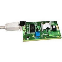
... INTERFACE PRINTED CIRCUIT BOARD (PCB) The ADIS16265/PCBZ includes one ADIS16265BCCZ 1.2 inch × 1.3 inch PCB. The ADIS16260/PCBZ includes one ADIS16260BCCZ on a 1.2 inch × 1.3 inch PCB. The interface PCB simplifies the IC connection of these devices to an existing processor system. The four mounting holes accommodate either M2 (2 mm) or 2-56 machine screws ...
Page 19
× 0.673 * i Sensor C1 2 × 0.000 0.150 * PIN 1 IDENTIFIER Figure 20. PCB Assembly View and Dimensions Rev Page ADIS16260/ADIS16265 J2 * ...
Page 20
... ORDERING GUIDE 1 Model Temperature Range ADIS16260BCCZ −40°C to +105°C ADIS16260/PCBZ ADIS16265BCCZ −40°C to +105°C ADIS16265/PCBZ RoHS Compliant Part. ©2009–2010 Analog Devices, Inc. All rights reserved. Trademarks and registered trademarks are the property of their respective owners. D08246-0-12/10(B) 7.600 BSC (4×) 3 ...