EVAL-ADUC7028QSZ Analog Devices Inc, EVAL-ADUC7028QSZ Datasheet - Page 6
EVAL-ADUC7028QSZ
Manufacturer Part Number
EVAL-ADUC7028QSZ
Description
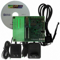
KIT DEV ADUC7028 QUICK START
Manufacturer
Analog Devices Inc
Series
QuickStart™ Kitr
Type
MCUr
Specifications of EVAL-ADUC7028QSZ
Contents
Evaluation Board, Power Supply, Cable, Software and Documentation
For Use With/related Products
ADuC7028
Lead Free Status / RoHS Status
Lead free / RoHS Compliant


ADuC7019/20/21/22/24/25/26/27/28/29
SPECIFICATIONS
AV
Table 1.
Parameter
ADC CHANNEL SPECIFICATIONS
ENDPOINT ERRORS
DYNAMIC PERFORMANCE
ANALOG INPUT
ON-CHIP VOLTAGE REFERENCE
EXTERNAL REFERENCE INPUT
DAC CHANNEL SPECIFICATIONS
ANALOG OUTPUTS
Output Voltage Range_2
Output Impedance
ADC Power-Up Time
DC Accuracy
Resolution
Integral Nonlinearity
Differential Nonlinearity
DC Code Distribution
Offset Error
Offset Error Match
Gain Error
Gain Error Match
Signal-to-Noise Ratio (SNR)
Total Harmonic Distortion (THD)
Peak Harmonic or Spurious Noise
Channel-to-Channel Crosstalk
Input Voltage Ranges
Leakage Current
Input Capacitance
Output Voltage
Accuracy
Reference Temperature Coefficient
Power Supply Rejection Ratio
Output Impedance
Internal V
Input Voltage Range
DC Accuracy
Output Voltage Range_0
Output Voltage Range_1
DD
(PHSN)
Differential Mode
Single-Ended Mode
Resolution
Relative Accuracy
Differential Nonlinearity
Offset Error
Gain Error
Gain Error Mismatch
= IOV
REF
DD
Power-On Time
8
= 2.7 V to 3.6 V, V
1, 2
7
5
3, 4
REF
= 2.5 V internal reference, f
Min
12
0.625
Typ
5
±0.6
±1.0
±0.5
+0.7/−0.6
1
±1
±1
±2
±1
69
−78
−75
−80
±1
20
2.5
±40
75
70
1
12
±2
0.1
0 to DAC
0 to 2.5
0 to DACV
2
REF
DD
Rev. C | Page 6 of 96
CORE
Max
±1.5
+1/−0.9
±2
±5
V
0 to V
±6
±5
AV
±1
±15
±1
CM
DD
6
= 41.78 MHz, T
± V
REF
REF
/2
Unit
μs
Bits
LSB
LSB
LSB
LSB
LSB
LSB
LSB
dB
dB
dB
V
V
μA
pF
V
mV
ppm/°C
dB
ms
V
Bits
LSB
LSB
mV
%
V
V
Ω
LSB
LSB
dB
Ω
%
V
A
= −40°C to +125°C, unless otherwise noted.
Eight acquisition clocks and fADC/2
% of full scale on DAC0
Test Conditions/Comments
2.5 V internal reference
1.0 V external reference
2.5 V internal reference
1.0 V external reference
ADC input is a dc voltage
f
Includes distortion and noise components
Measured on adjacent channels
During ADC acquisition
0.47 μF from V
T
T
R
Guaranteed monotonic
2.5 V internal reference
DAC
IN
A
A
L
= 5 kΩ, C
= 10 kHz sine wave, f
= 25°C
= 25°C
REF
range: DACGND to DACV
L
= 100 pF
REF
to AGND
SAMPLE
= 1 MSPS
DD
Related parts for EVAL-ADUC7028QSZ
Image
Part Number
Description
Manufacturer
Datasheet
Request
R

Part Number:
Description:
IC, ADJ LDO REG, 1.5V TO 5V 250mA MSOP-8
Manufacturer:
Vishay
Datasheet:

Part Number:
Description:
IC, ADJ LDO REG, 1.5V TO 5V 0.6A 8-TSSOP
Manufacturer:
Vishay
Datasheet:
Part Number:
Description:
IC, ADJ LDO REG, 1.5V TO 5V 250mA MSOP-8
Manufacturer:
Vishay
Datasheet:

Part Number:
Description:
IC ADJ LDO REG 1.5V TO 5V 150mA 5-SOT-23
Manufacturer:
Vishay
Datasheet:

Part Number:
Description:
BOARD EVAL AS1324-AD
Manufacturer:
austriamicrosystems
Datasheet:
Part Number:
Description:
IC, ADJ LDO REG, 1.5V TO 5V 0.6A 8-TSSOP
Manufacturer:
Vishay
Datasheet:

Part Number:
Description:
IC, ADJ LDO REG, 1.5V TO 5V, 0.3A, MSOP8
Manufacturer:
Vishay
Datasheet:
Part Number:
Description:
IC, ADJ LDO REG, 1.5V TO 5V, 0.3A, MSOP8
Manufacturer:
Vishay
Datasheet:
Part Number:
Description:
IC, ADJ LDO REG 1.215V TO 5V 0.3A MSOP-8
Manufacturer:
Vishay
Datasheet:
Part Number:
Description:
IC, ADJ LDO REG 1.215V TO 5V 0.3A MSOP-8
Manufacturer:
Vishay
Datasheet:

Part Number:
Description:
±1.7g Dual-Axis IMEMS Accelerometer Evaluation Board
Manufacturer:
Analog Devices Inc
Datasheet:

Part Number:
Description:
IC MULTIPLIER ANALOG 8-SOIC T/R
Manufacturer:
Analog Devices Inc
Datasheet:

Part Number:
Description:
IC ANALOG MULTIPLIER 8-DIP
Manufacturer:
Analog Devices Inc
Datasheet:
Part Number:
Description:
IC ANALOG MULTIPLIER 8-SOIC
Manufacturer:
Analog Devices Inc
Datasheet:
Part Number:
Description:
IC ANALOG MULTIPLIER 8-DIP
Manufacturer:
Analog Devices Inc
Datasheet: